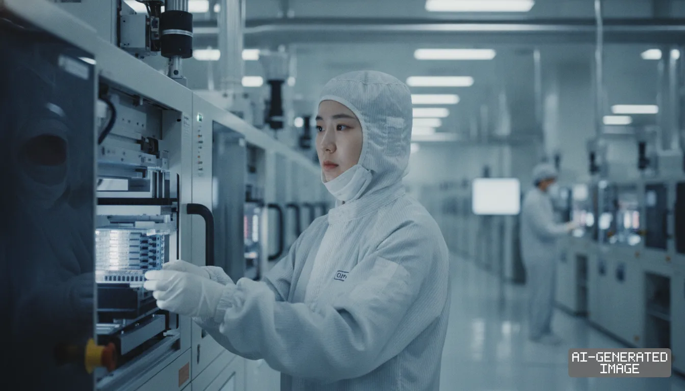
LG taps Samsung Foundry for appliance AI chips under Korean state project
The 31 billion won development consortium marks a rare shift by LG away from TSMC as Seoul backs domestic edge processor supply chains.

Business•Industry•Policy Intelligence
Memory, foundry, equipment and materials across Korea, China and Japan — and the export rules that bound them.
The 31 billion won development consortium marks a rare shift by LG away from TSMC as Seoul backs domestic edge processor supply chains.
The Japanese components maker completed construction of its Isahaya site on Sept.
State-backed R&D programs and fab equipment vendors target ultra-thin capacitor films with dielectric constants above 100 for…
Automotive suppliers integrate high-voltage power management silicon into domestic 300mm foundry lines to secure electrified…
Philoptics, EO Technics and LG Electronics deploy laser drilling tools as packaging makers validate glass cores for AI chiplets.
JSR, TOK and Adeka advance inorganic patterning materials as leading foundries test sub-2nm lines on ASML 0.55 NA scanners.
Advanced packaging suppliers across South Korea, Japan, and China target metal-diamond substrates and engineered TIMs to clear…
Furukawa Electric and Sumitomo Electric expand continuous-wave laser output as data centers adopt external optical sources.
Hybrid bonding and ultra-thin interposers reshape advanced packaging supply chains as fabless AI accelerator designers navigate…
Japanese metrology specialist Lasertec and Finland's Canatu integrate dedicated CNT pellicle inspection systems to secure…

East Asian chip designers and memory manufacturers begin sampling PCIe 6.2 controllers and switches to scale AI server memory…
Commercial co-packaged optics platforms from TSMC, Samsung, and Tower target interconnect bottlenecks and thermal limits across…
Japanese toolmakers secure process-of-record status on advanced logic pilot lines as backside power delivery doubles lithography…
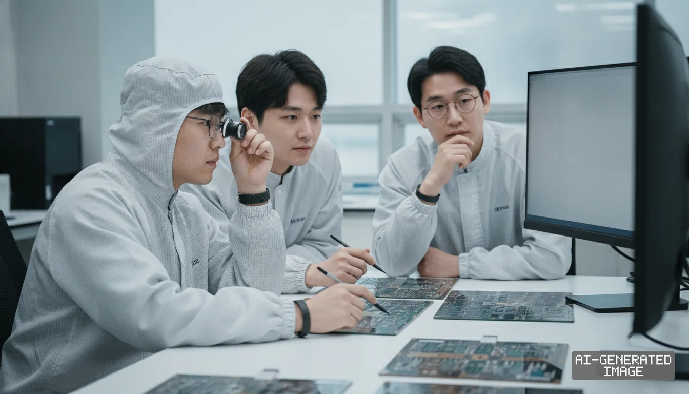
LG Innotek and Samsung Electro-Mechanics advance bridge-embedded FC-BGA substrates to lower 2.5D packaging costs for AI…
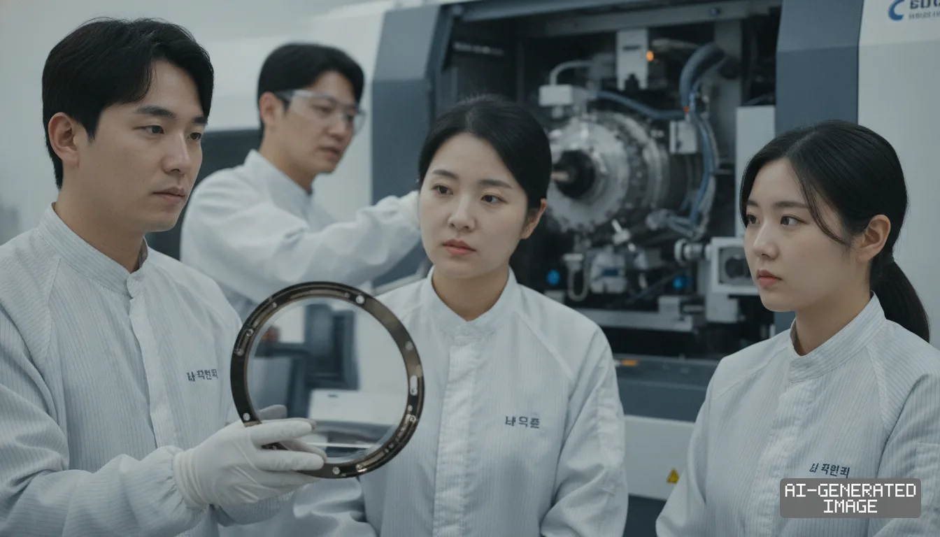
HOYA and AGC accelerate extreme low thermal expansion blank deliveries to foundries and R&D consortia as High-NA EUV lithography…
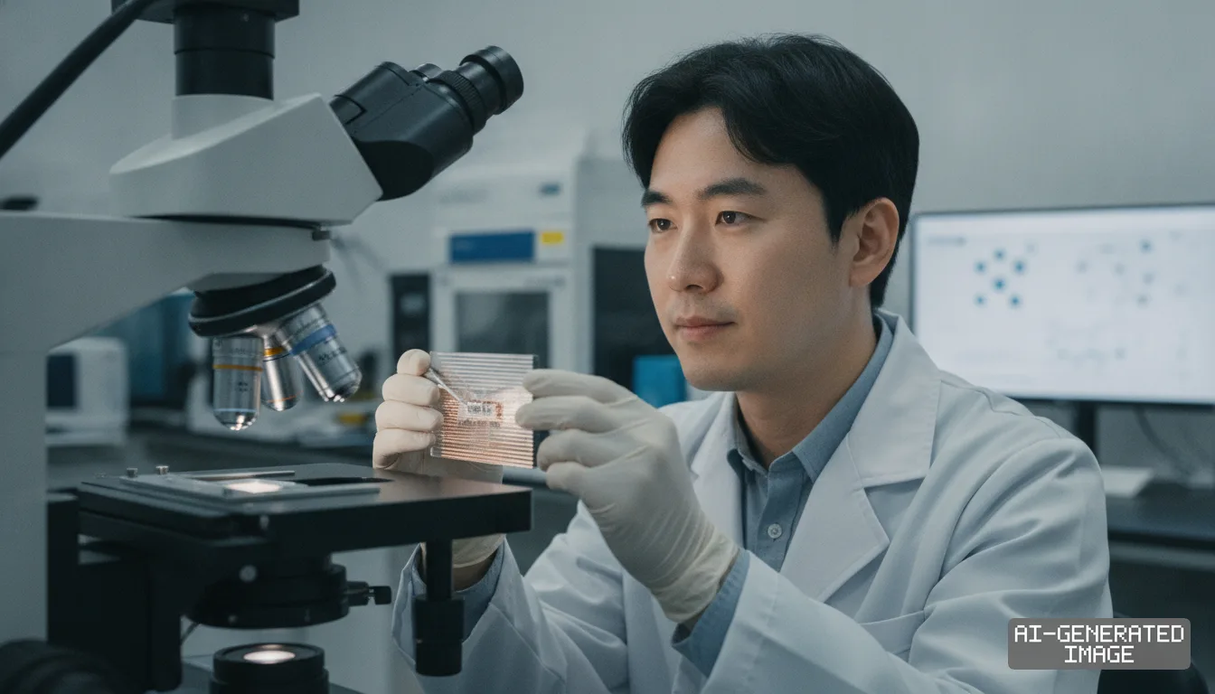
Chemical suppliers modify spherical silica filler morphology and polymer matrices to counter extreme thermomechanical stress…
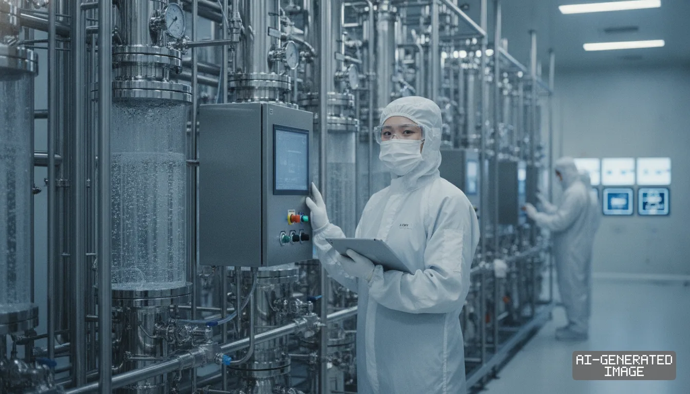
Domestic specialty producers scale distillation systems and validation protocols to supply 5N-grade fluorocarbons directly to…
DB HiTek and SK keyfoundry reallocate mature 200mm wafer capacity toward high-voltage automotive power management ICs to counter…
Chinese fabless designers are taping out custom RISC-V edge accelerators on SMIC 14nm lines to bypass advanced packaging…

The trade ministry establishes dedicated testbeds and research grants to close back-end gaps and scale next-generation wafer…
China's largest OSAT is ramping high-density system-in-package capacity for 77 GHz millimeter-wave modules at its Jiangyin plant.
The Korean chipmaker is reallocating 200mm and trailing 300mm fab lines toward BCD and microcontroller processes to defend fab…
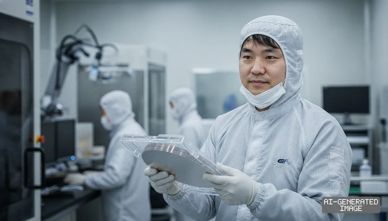
Domestic wafer manufacturers scale 12-inch polished and epitaxial shipments to supply local foundries, displacing imported…
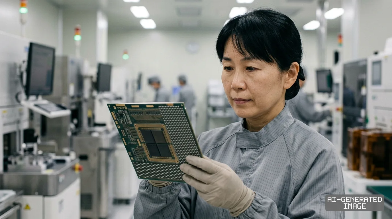
Japanese substrate leaders accelerate volume production at new domestic facilities to meet multi-chip packaging demand from…