Kyocera opens 68 billion yen Nagasaki plant for AI chip packaging
The Japanese components maker completed construction of its Isahaya site on Sept. 1, targeting 25 billion yen in annual capacity for AI hardware by 2030.
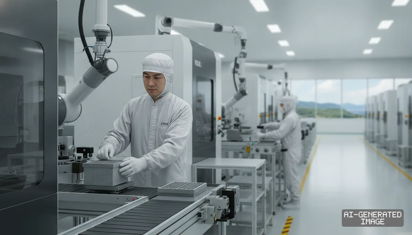
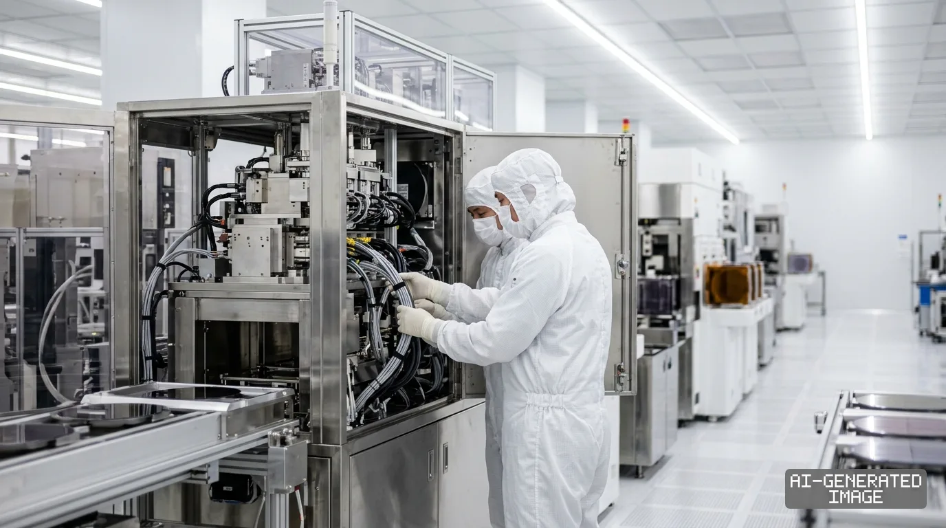
Kyocera completed construction of its 68 billion yen ($465 million) semiconductor component facility in Nagasaki on Sept. 1, 2026. The site will manufacture packaging substrates and ceramic parts for artificial intelligence hardware.
The Kyoto-based manufacturer held a completion ceremony Tuesday morning at the Nagasaki Isahaya Plant. Company executives confirmed that equipment installation will proceed in stages ahead of commercial production in spring 2027.
The facility represents Kyocera's largest domestic factory addition in nearly two decades. Kyocera designs ceramic casings and multi-layer packaging substrates that house high-performance computing processors and power semiconductors.
Kyocera acquired the 150,000-square-meter site within the Minami Isahaya Industrial Park across two purchase agreements concluded between 2023 and 2024. The complex features a six-story steel structure with 80,799 square meters of total floor space.
The company scheduled capital expenditures of 68 billion yen across the site through March 2029. Kyocera set an annual production output target of 25 billion yen ($171 million) from the plant starting in the fiscal year ending March 31, 2030.
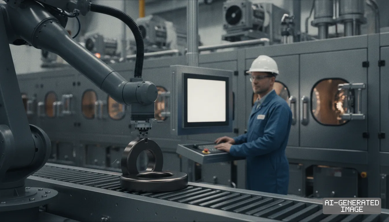
Production will center on two primary product lines. The plant will fabricate high-purity fine ceramic structural components used in semiconductor fabrication tools such as etching chambers and wafer stages. It will also produce ceramic packages for advanced driver-assistance systems, electric vehicles and AI data center accelerators.
Fine ceramics withstand extreme thermal loads and plasma corrosion during advanced node wafer processing. Japanese component makers supply the majority of the precision structural ceramics used by global lithography and deposition toolmakers.
Advanced packaging has emerged as a critical manufacturing choke point as chip designers connect multiple chiplets on shared substrates. Thermal expansion mismatches between silicon dies and organic boards have prompted broader adoption of rigid ceramic bases.
Kyocera appointed Naotaka Oota as plant manager effective Sept. 1, following an initial management notice published on July 1. Kyocera President Shiro Sakushima led the opening event alongside corporate directors in Isahaya.
Kyocera first announced its intent to build the Nagasaki plant in December 2022 to resolve floor space constraints at its existing manufacturing hubs in Kagoshima and Shiga. Kyocera signed the formal land acquisition agreement with Nagasaki Prefecture and Isahaya City in April 2023.
The company broke ground on the factory in August 2024, completing the main structure in 24 months. The company said the facility will create local manufacturing jobs while securing component delivery schedules for international semiconductor equipment manufacturers.
Kyocera operates packaging and fine ceramics lines across Japan, Southeast Asia and the United States. The Isahaya hub consolidates advanced substrate manufacturing closer to foundry clusters across Kyushu.
Kyocera will begin trial runs on initial processing equipment later this year ahead of customer validation cycles scheduled for early 2027.
Impact map
How this development propagates across the region and out to global buyers.
| Event | Korea | China | Japan | Global impact |
|---|---|---|---|---|
| Nagasaki plant completion | — | — | ceramic and packaging output | AI hardware supply |
In this story
- Companies
- Kyocera
- Tickers
- 6971.T
- Impact
- CapexSupply Chain
Related briefings
Sources
Primary documents
Reporting
Confidence: high — how we grade this
The documents behind this briefing are linked above. East Asia Brief produces its English text with AI assistance under human editorial review, and does not translate or republish other outlets' articles. See our methodology and AI policy. Spotted an error? Tell us.
The Morning Brief
What changed in Korean, Chinese and Japanese industry overnight — and what it means for your supply chain. One email, weekday mornings, US time. Free.
The Morning Brief is in preparation. Leave your address and we will write to you once — when the first issue is ready. Nothing before that.