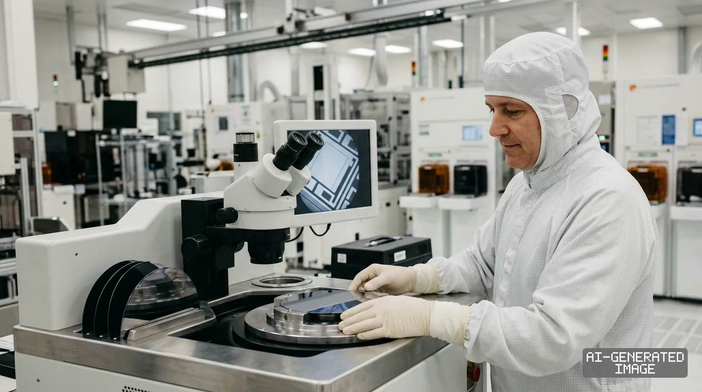
Samsung Foundry converts mature planar lines to automotive power chips
The Korean chipmaker is reallocating 200mm and trailing 300mm fab lines toward BCD and microcontroller processes to defend fab utilization.

Samsung Electronics has reallocated trailing-edge wafer fabrication lines at its Giheung and Hwaseong manufacturing complexes in South Korea, shifting mature planar capacity toward high-voltage power management integrated circuits and automotive microcontrollers. The operational adjustment converts legacy 200-millimeter and 300-millimeter production lines that previously manufactured display driver integrated circuits and commoditized consumer logic, redirecting production tools toward specialized Bipolar-CMOS-DMOS and embedded non-volatile memory processes.
The conversion targets fully depreciated manufacturing infrastructure, primarily 200-millimeter Line 6 at Giheung and select 300-millimeter planar lines at Hwaseong that run 28-nanometer, 65-nanometer, and 130-nanometer processes. By deploying updated process design kits for high-voltage power applications and industrial microcontrollers, Samsung Foundry aims to stabilize line utilization rates that softened following a broad cyclical slowdown in consumer electronics and aggressive mature-node capacity additions by contract foundries in mainland China.
Mainland Chinese foundries, including Semiconductor Manufacturing International Corporation, Hua Hong Semiconductor, and Nexchip Semiconductor, have brought online extensive 200-millimeter and 300-millimeter legacy capacity over the past three years. That capacity expansion concentrated in standard CMOS logic nodes between 55 nanometers and 180 nanometers, creating persistent downward pressure on spot foundry wafer prices for display driver ICs, image sensors, and consumer-grade logic. Reallocating lines toward power and automotive processes insulates Samsung from standard logic price competition, as these specialized platforms demand higher voltage tolerances and extended qualification periods that discourage rapid supplier switching.
In Giheung, Samsung has configured 200-millimeter Bipolar-CMOS-DMOS lines to support operating voltages ranging from 24 volts to 100 volts. These voltage thresholds are standard for power management chips used in enterprise server power supply units, industrial motor controllers, and automotive battery management systems. The BCD process allows analog control circuitry, high-voltage DMOS output transistors, and digital CMOS logic to reside on a single monolithic silicon die, reducing physical footprint and energy dissipation compared to multi-chip packaging solutions.
At the Hwaseong site, Samsung is transitioning trailing 300-millimeter capacity to 28-nanometer embedded magnetic random-access memory platforms. Integrating embedded MRAM into 28-nanometer planar microcontrollers allows automotive electronic control units to retain operational data without continuous power draw, while providing higher read and write endurance than conventional embedded flash memory. The 28-nanometer node represents the industry's most cost-effective planar transition point before switching to expensive three-dimensional FinFET transistor architectures.
The transition process requires retrofitting specific manufacturing steps on existing production floors rather than purchasing entirely new lithography tools. Samsung is installing specialized high-energy ion implanters, high-temperature thermal annealing furnaces, and thick-metal deposition equipment required for high-voltage power stages. Because the underlying argon fluoride and krypton fluoride deep-ultraviolet lithography tools are already fully depreciated, the marginal capital expenditure per wafer start remains low relative to greenfield semiconductor fab construction.
Automotive qualification requirements establish multi-year revenue stability once fab lines clear customer audits. Commercial components for automotive applications must meet AEC-Q100 Grade 0 and Grade 1 standards, requiring documented operation across ambient temperatures from minus 40 degrees to 150 degrees Celsius alongside zero-defect manufacturing parameters certified under ISO 26262 functional safety protocols. Fabless design houses and automotive Tier-1 suppliers typically commit to three-to-five-year wafer supply agreements once a specialized process node achieves qualification.
The strategic shift mirrors defensive adjustments executed across the contract manufacturing sector in Taiwan and South Korea. Pure-play foundries have differentiated legacy operations by investing in specialty analog, gallium nitride on silicon, and high-voltage process extensions. Taiwan Semiconductor Manufacturing Company has anchored its legacy 28-nanometer operations in specialty microcontroller and image signal processor lines, while South Korea's DB HiTek has expanded its 0.13-micron and 0.18-micron BCD offerings to protect gross margins against commoditized logic erosion.
Customer integration for Samsung's converted capacity includes domestic South Korean fabless designers and international automotive suppliers. South Korean power management design houses, including Silicon Mitus and LX Semicon, have qualified high-voltage BCD designs at Giheung to supply power delivery chips for domestic electric vehicle platforms and premium home appliances. International automotive Tier-1 component makers have engaged Samsung Foundry to dual-source power stage drivers and microcontroller silicon outside mainland China, mitigating geopolitical supply chain concentration risks.
The reallocation alters Samsung Foundry's operational revenue composition, lifting the proportion of industrial, power, and automotive wafer starts relative to mobile application processors and consumer electronics logic. Samsung Foundry is completing production audits for its 28-nanometer automotive embedded MRAM platform, with commercial volume shipments scheduled to ramp through the fourth quarter of 2026.
Impact map
How this development propagates across the region and out to global buyers.
| Event | Korea | China | Japan | Global impact |
|---|---|---|---|---|
| Foundry Mature Node Realignment | legacy line repurposing | price competition on standard logic | automotive MCU procurement | power IC supply diversification |
In this story
- Companies
- Samsung Electronics
- Tickers
- 005930.KS
- Exposed
- DB HitekHua Hong SemiconductorLX SemiconSilicon Mitus
- Policy
- Economic SecuritySubsidies
- Impact
- CapexSupply ChainPricingCost Structure
Track every Economic Security development → Track every Subsidies development →
Related briefings
- SMIC narrows foundry gap with Samsung as Q2 sales surge 20% Also on Hua Hong Semiconductor, Samsung Electronics, Pricing
- East Asia accelerates 8-inch silicon carbide capacity race as power chip makers scale output Also on DB Hitek, Pricing, Cost Structure
- Korea Foundries Shift 200mm Lines to Auto PMICs as EV Architectures Advance Also on DB HiTek, Pricing
- China expands 300mm silicon wafer capacity to cut reliance on Japanese suppliers Also on Hua Hong Semiconductor, Pricing
Sources
This briefing carries no sources block. It was written from our desks’ working knowledge of the sector rather than from documents retrieved for this piece. Read it as orientation and check any figure you intend to act on — how we source briefings.
This briefing carries no linked sources: it was written from our desks' working knowledge of the sector rather than from documents retrieved for this piece. East Asia Brief publishes no citation it cannot link. Our English text is produced with AI assistance under human editorial review. See our methodology and AI policy. Spotted an error? Tell us.
The Morning Brief
What changed in Korean, Chinese and Japanese industry overnight — and what it means for your supply chain. One email, weekday mornings, US time. Free.
The Morning Brief is in preparation. Leave your address and we will write to you once — when the first issue is ready. Nothing before that.