Japanese photoresist makers validate metal oxide resist lines for High-NA EUV chipmaking
JSR, TOK and Adeka advance inorganic patterning materials as leading foundries test sub-2nm lines on ASML 0.55 NA scanners.
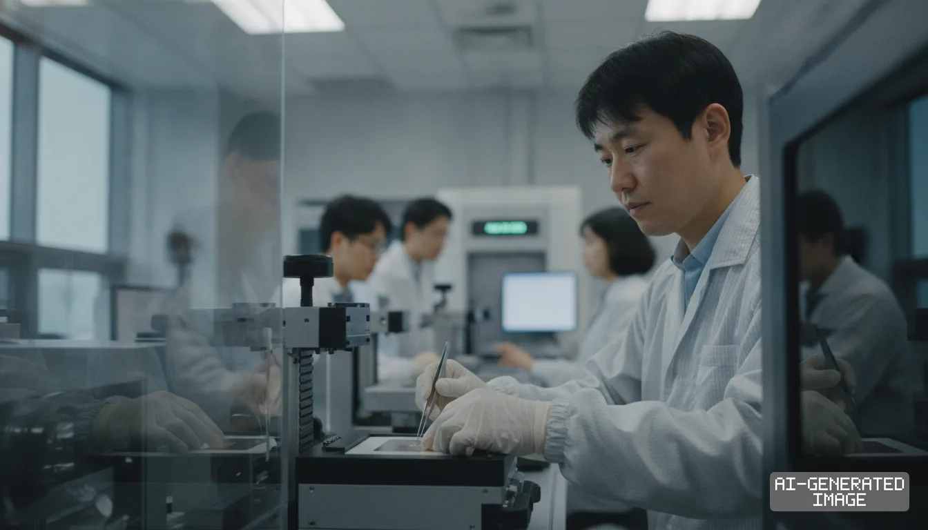
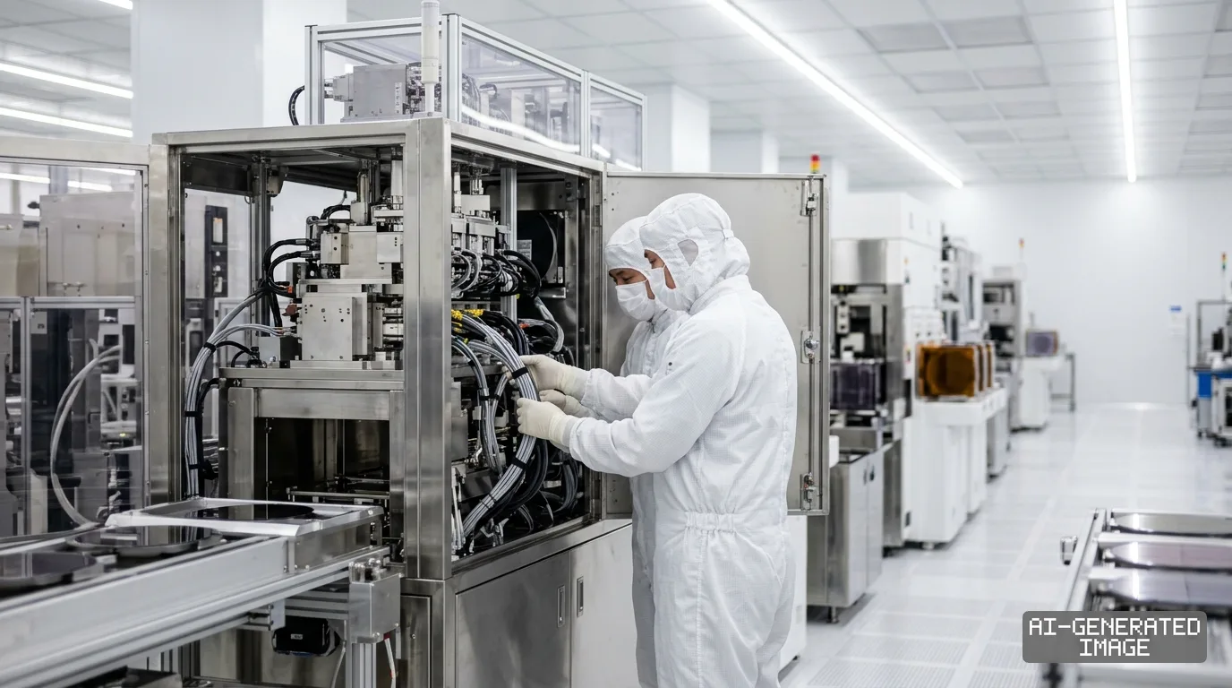
Japanese semiconductor materials suppliers accelerated commercial validation of inorganic metal oxide photoresists on Aug. 20, 2026, positioning new chemical formulations for commercial High-NA extreme ultraviolet lithography lines.
The shift addresses physical limits in conventional chemically amplified resists, which struggle to resolve sub-2nm circuit features on ASML high numerical aperture scanners.
High-NA EUV tools increase the optical numerical aperture from 0.33 to 0.55, allowing fabs to print finer features in a single exposure.
That higher resolution reduces the depth of focus, forcing foundries to coat wafers with significantly thinner photoresist layers to prevent pattern collapse.
Thinner organic films capture fewer EUV photons per unit area.
This photon shot noise triggers stochastic defects — random bridge contacts, line breaks and critical dimension variations across the wafer.
Metal oxide resists replace carbon-based polymer backbones with tin-based inorganic molecular clusters.
Tin atoms possess a much higher EUV photon absorption cross-section than carbon or hydrogen, absorbing between two and four times more light at the 13.5-nanometer wavelength.
Because metal oxide resists react directly with photons without relying on photoacid generator diffusion, they eliminate acid blur and cut stochastic defects.
The resulting inorganic pattern also delivers superior etch resistance, enabling cleaner transfers into underlying hardmask layers.
JSR Corporation established an early foothold in this segment by acquiring United States developer Inpria Corporation in September 2021.
The company is preparing to start trial runs at a dedicated commercial metal oxide resist plant under JSR Micro Korea by late 2026.
To solve deposition and development challenges, JSR and Inpria signed a non-exclusive cross-licensing pact with Lam Research on Sept. 15, 2025.
The agreement couples JSR material chemistries with Lam's dry resist deposition and dry development equipment platform, called Aether.
Dry resist processing applies the metal oxide film inside a vacuum chamber via chemical vapor deposition rather than standard wet spin-coating.
That vacuum approach reduces chemical waste, improves coating uniformity on thin profiles and avoids solvent striation defects on large 300-millimeter wafers.
Tokyo Ohka Kogyo, which holds roughly 29% of the global market for conventional EUV resists, is pursuing an alternative route.
The company signed a strategic investment and joint development agreement with Britain-based Irresistible Materials on Feb. 23, 2026.
The partnership commercializes Multi-Trigger Resist technology, a non-chemically amplified chemistry designed to yield high sensitivity with low line-edge roughness.
The formulation acts as a non-metal alternative intended to work on existing wet spin-track infrastructure without requiring vacuum deposition tool retrofits.
Adeka Corporation joined the supply buildout by breaking ground on a dedicated plant for organometallic compounds at its Kashima site in Kamisu, Ibaraki Prefecture.
The 3.2 billion yen ($20 million) project, approved on Oct. 31, 2025, targets commercial volume production by April 2028.
Adeka's Kashima lines synthesize organometallic precursor molecules that serve as key raw materials for both wet-applied and dry-deposited metal oxide formulations.
The supplier also commissioned its Semiconductor Innovation Center in Kuki City, Saitama Prefecture, in July 2026 to speed qualification cycles for bound photoacid generators.
Testing is centered at the joint imec-ASML High-NA EUV Test Center in Veldhoven, Netherlands, utilizing the EXE:5000 scanner.
Process engineers at Intel, Taiwan Semiconductor Manufacturing Co. and Samsung Electronics are running parallel evaluations of both spin-on and dry-deposited metal oxide resists.
The materials are being assessed for critical layers on Intel 14A, TSMC A16 and Samsung 2-nanometer foundry nodes.
Widespread deployment still faces commercial friction inside high-volume manufacturing facilities.
Inorganic resists introduce tin contamination risks into standard fab front-end lines, requiring segregated exhaust systems, dedicated tracks and tailored strip chemistries.
Metal oxide resists also carry higher raw chemical procurement costs per liter than standard chemically amplified resists.
Foundry operators weigh these chemical cost premiums against the yield gains achieved by cutting defect rates and avoiding multiple patterning passes.
Final volume supply contracts and binding allocation commitments remain protected under customer non-disclosure agreements.
ASML plans to begin shipping commercial-grade EXE:5200 high-volume scanners with productivity targets exceeding 200 wafers per hour starting in 2027.
Impact map
How this development propagates across the region and out to global buyers.
| Event | Korea | China | Japan | Global impact |
|---|---|---|---|---|
| High-NA EUV resist transition | foundries qualify inorganic resist lines | — | chemical makers build MOR capacity | lithography tool efficiency and yield gains |
In this story
- Companies
- JSR CorporationTokyo Ohka KogyoAdeka Corporation
- Tickers
- 4185.T4186.T4401.T
- Exposed
- ASMLLam ResearchTSMCIntelSamsung Electronics
- Policy
- Economic SecuritySubsidies
- Impact
- Supply ChainCapexCost Structure
Track every Economic Security development → Track every Subsidies development →
Related briefings
- TOK completes $76M chip chemical plant in Pyeongtaek, Korea Also on Tokyo Ohka Kogyo, Samsung Electronics, Subsidies
- JSR opens South Korea EUV photoresist plant for 2nm chips Also on JSR Corporation, Samsung Electronics, Subsidies
- Fujifilm plans $83 million chip materials plant in India Also on JSR Corporation, Subsidies
- ASML expands Japan workforce to 700 to support Rapidus 2nm and TSMC fabs Also on Lam Research, ASML, Cost Structure
Sources
Reporting
Confidence: medium — how we grade this
The documents behind this briefing are linked above. East Asia Brief produces its English text with AI assistance under human editorial review, and does not translate or republish other outlets' articles. See our methodology and AI policy. Spotted an error? Tell us.
The Morning Brief
What changed in Korean, Chinese and Japanese industry overnight — and what it means for your supply chain. One email, weekday mornings, US time. Free.
The Morning Brief is in preparation. Leave your address and we will write to you once — when the first issue is ready. Nothing before that.