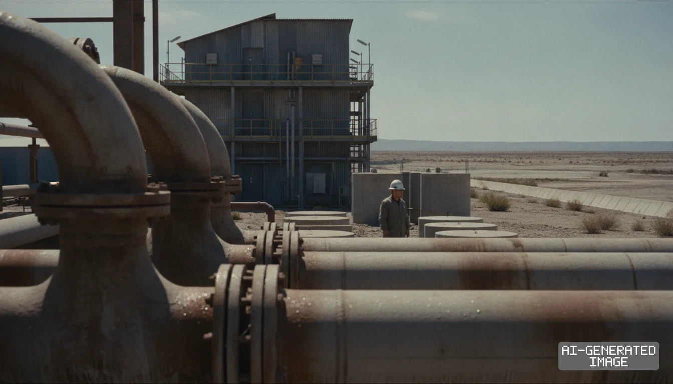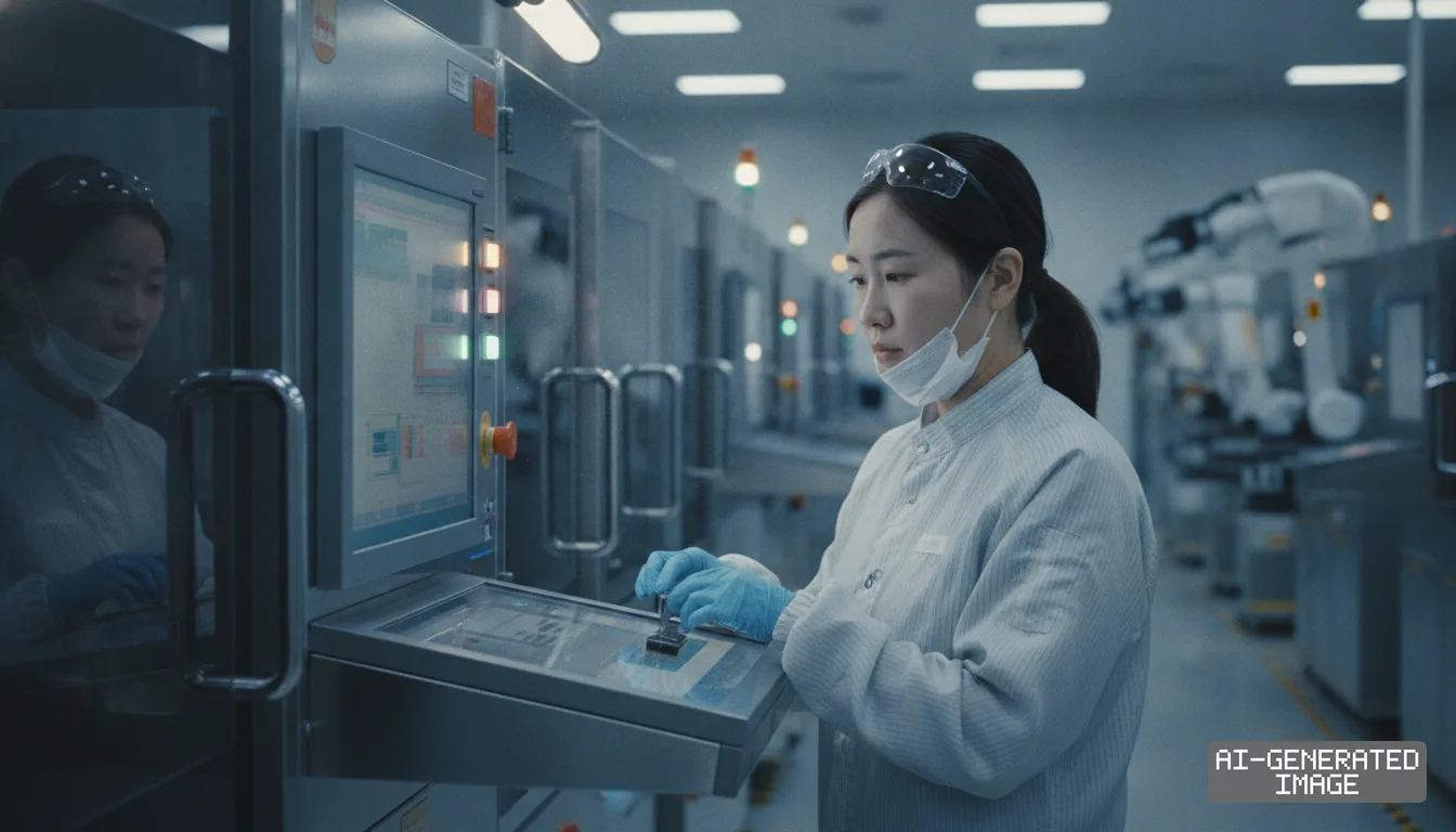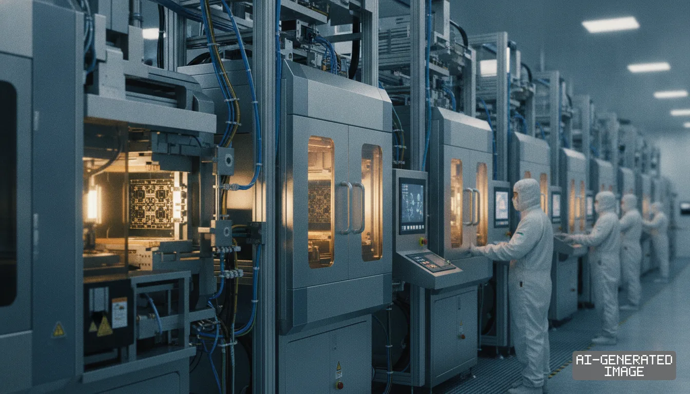
TSMC reviews vertical 3D DRAM production after Nvidia request
The foundry reviews dedicated lines to ease high-bandwidth memory shortages after advanced nodes generated 74% of its wafer revenue in 2025.
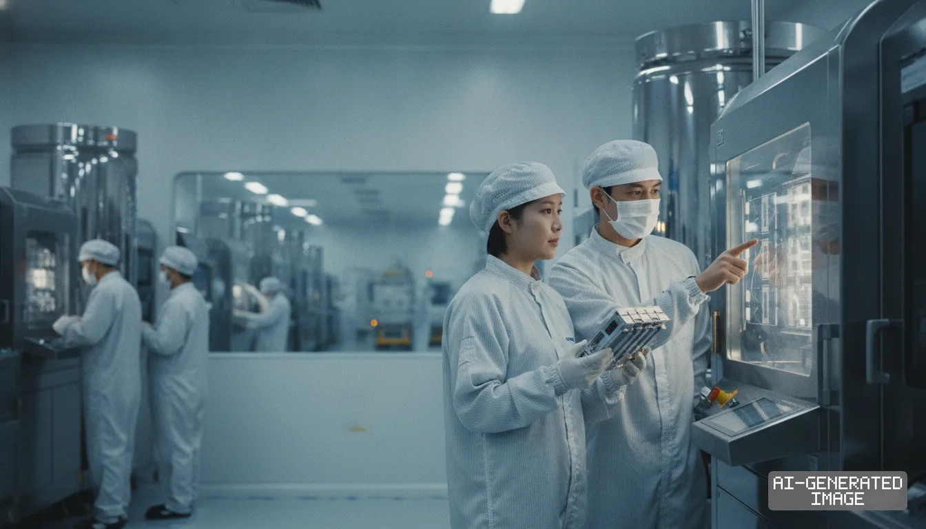
Taiwan Semiconductor Manufacturing Co. began evaluating options to manufacture vertical 3D DRAM on Nov. 6, 2026, following a formal request from its largest artificial intelligence client, Nvidia.
TSMC managed annual fabrication capacity exceeding 17 million 12-inch equivalent wafers in 2025. Advanced nodes at seven nanometers and below accounted for 74% of its total wafer revenue during that period.
Nvidia asked the contract chipmaker to establish dedicated memory lines to alleviate chronic supply constraints in high-bandwidth memory (HBM). Neither company has published an official capital commitment figure for the manufacturing project.
The feasibility review examines two operational pathways: constructing a greenfield fabrication facility or acquiring and converting an existing plant. Hsu Kuo-chin, vice president of advanced packaging at TSMC, leads the internal evaluation team.
A direct move into memory fabrication would mark a historic shift for TSMC. The company has operated exclusively as a pure-play logic foundry since its founding in 1987, avoiding direct competition with memory makers.
The prospective entry threatens to reshape the global memory oligopoly. South Korean chipmakers Samsung Electronics and SK hynix currently control approximately 85% of the worldwide DRAM market.
SK hynix holds more than 50% of the high-bandwidth memory sector. The company supplies the majority of the stacked DRAM modules integrated into Nvidia's flagship datacenter graphic processing units.
Samsung Electronics commands roughly 40% of the broader DRAM market. The company operates both contract foundry lines and memory fabrication plants across South Korea and the United States.
Micron Technology also faces direct exposure as the third major memory supplier. Micron holds about 20% of the DRAM market and paid $1.8 billion to acquire a manufacturing site in Taiwan to expand advanced memory lines.
High-bandwidth memory bundles multiple DRAM dies vertically on a silicon interposer. The assembly connects directly to logic processors through TSMC's proprietary Chip-on-Wafer-on-Substrate (CoWoS) packaging process.
Production bottlenecks in both HBM assembly and advanced packaging have constrained Nvidia accelerator shipments throughout 2025 and 2026. Delivery lead times for completed AI server modules have stretched past 40 weeks.
The architectural concept under review differs fundamentally from conventional packaging integration. Planar DRAM arrays store electrical charges in capacitors arranged side by side across a single silicon surface.
In contrast, 3D DRAM stacks individual storage cells vertically within a single monolithic memory array. The design multiplies cell density per square millimeter while shortening electrical signal distances.
Direct vertical integration reduces parasitic capacitance and lowers operating thermal loads. The architecture allows processors and memory arrays to exchange data without traversing external packaging substrates.
TSMC has developed foundational intellectual property for vertical memory structures over several years. The foundry filed patent applications for high-density 3D DRAM architectures in 2020 and published vertical-channel capacitor designs in 2025.
The company has also refined physical stacking technologies. In its 2025 annual report, TSMC disclosed stable production yields for wafer-on-wafer bonding, an advanced technique that attaches memory wafers to logic dies using 55-nanometer process technology.
Nvidia has expanded efforts to influence memory manufacturing architectures. The chip designer previously urged its primary memory suppliers to adopt TSMC's 3-nanometer logic node for the base dies of custom next-generation HBM stacks.
A dedicated TSMC memory fab would permit Nvidia to bypass conventional DRAM procurement entirely. Securing proprietary memory lines would insulate the processor designer from recurring industry shortages and quarterly price negotiations.
For TSMC, entering commercial memory production carries substantial execution and financial risks. Memory fabrication requires dedicated tool configurations, distinct chemical handling systems and continuous billions of dollars in annual capital expenditures.
Operating margins in pure-play logic foundries consistently exceed those of cyclical commodity memory manufacturers. Memory producers regularly endure sharp market downturns when consumer hardware demand weakens.
TSMC addressed the review on Nov. 6, 2026, reiterating its corporate focus. TSMC said it does not comment on market rumors and speculations, maintaining that it remains dedicated to its core logic foundry operations.
Nvidia declined to comment on discussions regarding memory manufacturing. Neither company has submitted regulatory disclosure filings to the Taiwan Stock Exchange or the US Securities and Exchange Commission regarding the project.
The preliminary review does not state whether TSMC would pursue joint development with an existing memory producer, and neither firm has published target wafer run-rates or production schedules.
The Taiwan Stock Exchange mandates immediate public disclosures for capital equipment acquisitions or joint-venture commitments exceeding statutory capital thresholds. TSMC management is scheduled to present its finalized capital budget during its annual investor conference in January 2027.
Impact map
How this development propagates across the region and out to global buyers.
| Event | Korea | China | Japan | Global impact |
|---|---|---|---|---|
| TSMC evaluates 3D DRAM manufacturing | Samsung and SK hynix face structural threat to 85% DRAM share and HBM pricing power | Memory makers face wider architectural gap if TSMC pairs 3D DRAM with advanced logic | Memory materials and vertical etch equipment suppliers gain secondary order pipeline | Nvidia secures potential alternative to three-firm memory oligopoly for AI accelerators |
In this story
- Companies
- Taiwan Semiconductor Manufacturing Co.Nvidia
- Tickers
- TSMNVDA
- Exposed
- Samsung ElectronicsSK hynixMicron Technology
- Impact
- Supply ChainCapexOrder Book
Related briefings
- Samsung Electronics opens HBM4 base die supply to rival TSMC for AI Also on Taiwan Semiconductor Manufacturing Co., Micron Technology, Nvidia
- Micron unveils vertical HBM architecture to stack on AI GPUs Also on Taiwan Semiconductor Manufacturing Co, Micron Technology, Nvidia
- TSMC widens CoWoS supply chain with $2 billion US interposer deal Also on Taiwan Semiconductor Manufacturing Co., Nvidia, SK hynix
- GlobalFoundries agrees to build silicon interposers for TSMC in $2B deal Also on Taiwan Semiconductor Manufacturing Co., Nvidia, SK hynix
Sources
Primary documents
Reporting
Confidence: high — how we grade this
The documents behind this briefing are linked above. East Asia Brief produces its English text with AI assistance under human editorial review, and does not translate or republish other outlets' articles. See our methodology and AI policy. Spotted an error? Tell us.
The Morning Brief
What changed in Korean, Chinese and Japanese industry overnight — and what it means for your supply chain. One email, weekday mornings, US time. Free.
The Morning Brief is in preparation. Leave your address and we will write to you once — when the first issue is ready. Nothing before that.