Nvidia aligns TSMC and memory makers to ease 20% packaging shortfall
The coordination framework synchronizes five countries to break Blackwell delivery logjams as Nvidia absorbs 60% of TSMC's 130,000 monthly packaging wafers.
Nvidia activated a multilateral production coordination framework with foundry, substrate and memory suppliers on Nov. 6, 2026, targeting advanced packaging bottlenecks that constrain its Blackwell AI accelerator deliveries.
The coordinated effort links contract fabricator Taiwan Semiconductor Manufacturing Company with Japanese packaging specialists and South Korean memory producers. The companies intend to synchronize component staging across five countries.
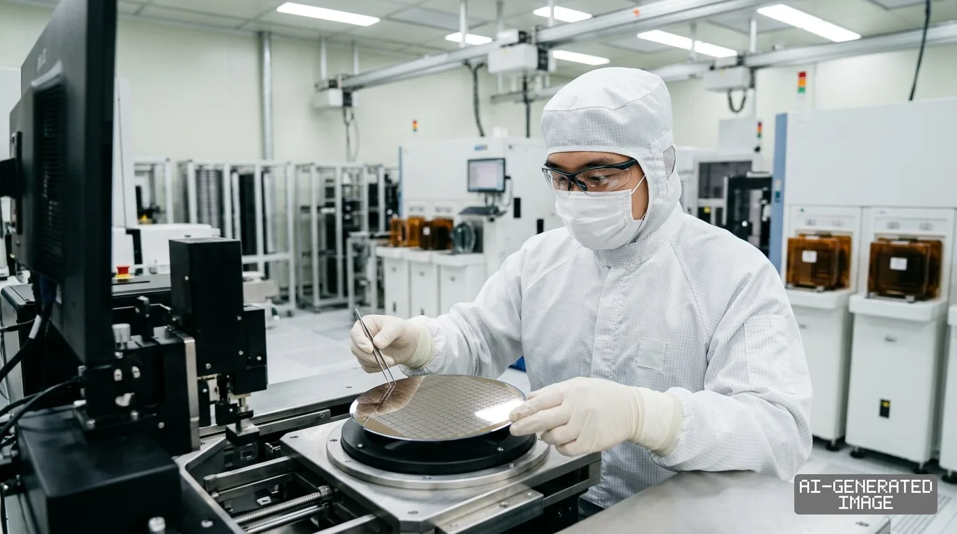
The coordinated push addresses an estimated 20% supply shortfall across TSMC's Chip-on-Wafer-on-Substrate lines. The foundry operates roughly 130,000 packaging wafers per month, with Nvidia commanding about 60% of that total output.
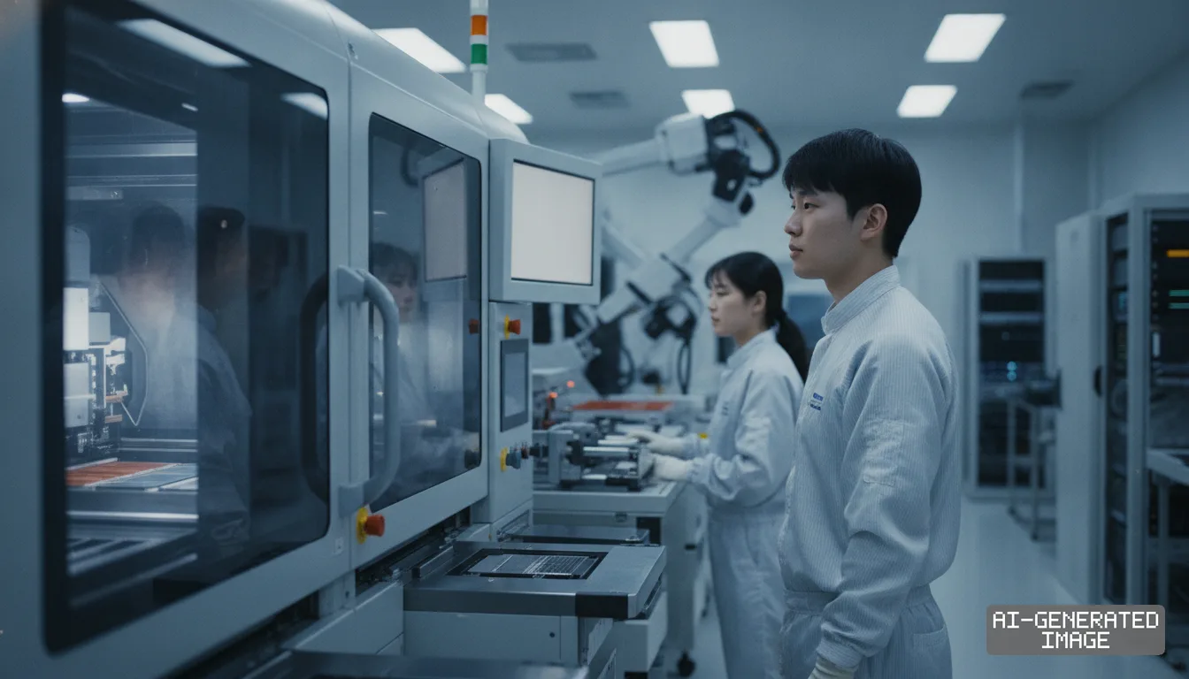
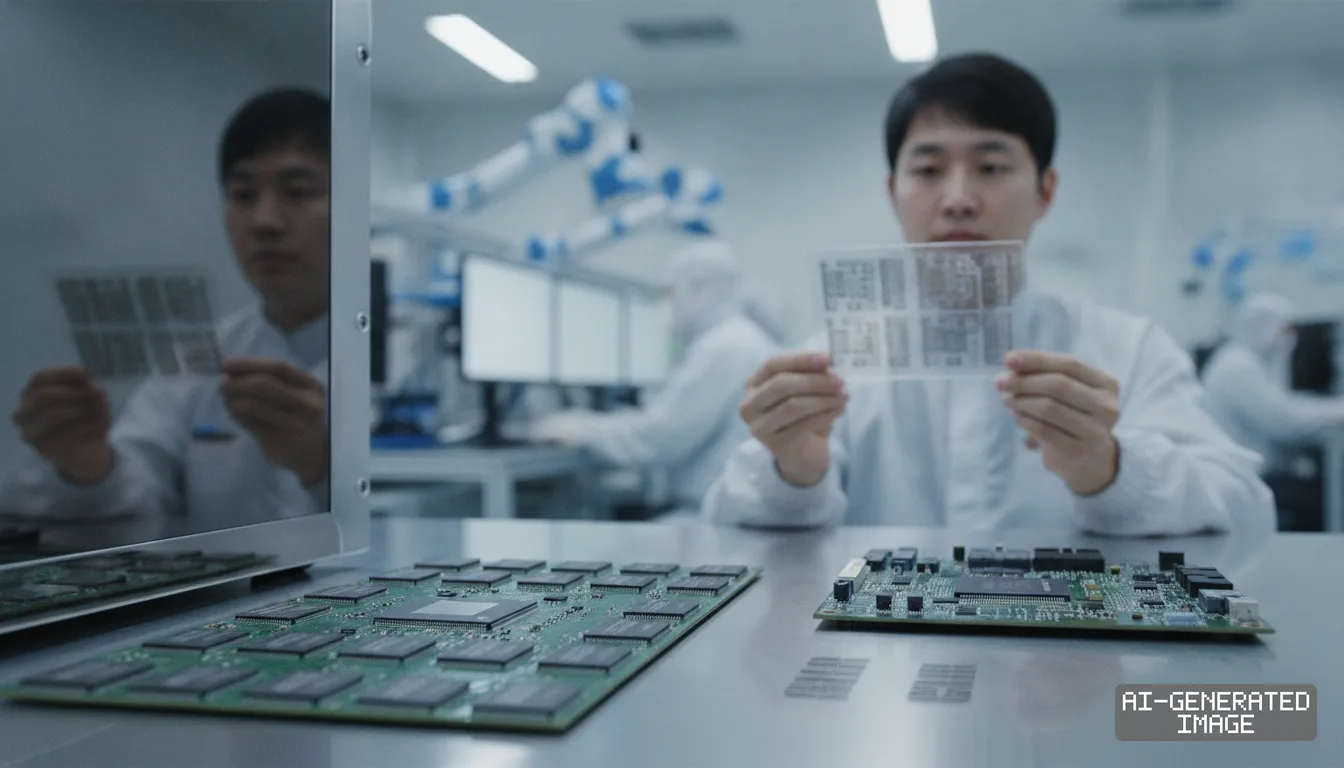
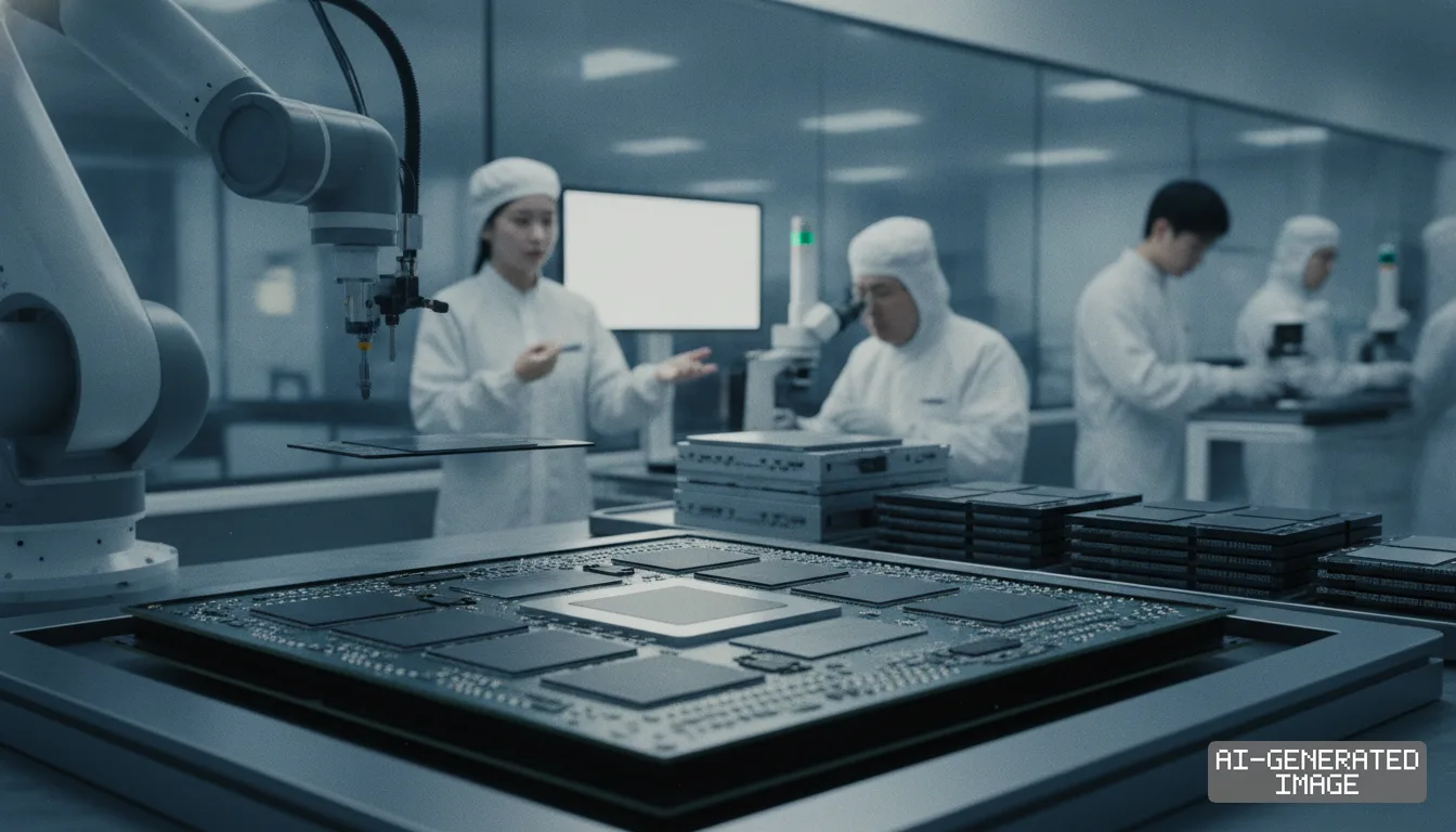
Backend packaging has replaced front-end wafer fabrication as the main production constraint for leading-edge artificial intelligence hardware. The Blackwell architecture packages two high-performance computing dies alongside eight high-bandwidth memory stacks on a single module.
TSMC packages these multi-die processors using its CoWoS-L process, which embeds local silicon interconnects inside an organic redistribution layer. The complex structure requires significantly larger interposers than earlier accelerator designs, reducing total finished units per wafer.
Equipment lead times for advanced packaging tools now stretch to eight months, company filings show. The extended delivery cycle has limited TSMC from accelerating line installations at its backend packaging facilities in Taiwan.
TSMC has expanded its capital expenditure for advanced packaging to $12.4 billion, company financial disclosures show. The foundry plans to double its monthly packaging throughput to 260,000 wafers by 2028.
To ease the immediate crunch, TSMC has outsourced secondary assembly steps to OSAT partners including ASE Technology Holding and Amkor. ASE handles wafer-on-substrate bonding, which accounts for roughly 15% of total backend processing steps.
Japanese substrate supplier Ibiden has committed dedicated production capacity from its domestic manufacturing lines. High-performance computing substrates account for more than 40% of Ibiden's packaging material sales, company reports show.
Ajinomoto supplies the specialized build-up film that insulates the high-density wiring layers inside each package. The Tokyo-based chemical firm produces nearly 90% of the world's dielectric film used in advanced semiconductor packaging.
South Korean memory producer SK hynix provides the primary volume of eight-stack HBM3E memory modules for the Blackwell platform. The company dedicated over 50% of its high-bandwidth memory capacity to long-term supply agreements.
Samsung Electronics has begun qualification runs to expand its secondary supply allocation for next-generation packaging lines. The memory maker seeks to capture up to 30% of supplementary HBM shipments for upcoming accelerator revisions.
Data center operators have experienced delivery backlogs extending past six months for complete server racks. Cloud infrastructure providers require schedule predictability as enterprise customers expand large language model training and inference clusters.
The multilateral production framework establishes unified quality metrics across materials, memory bonding and thermal testing. Participating suppliers will exchange daily throughput logs through a secure production data bridge to spot component imbalances.
Testing procedures for Blackwell processors require three to four times longer than previous-generation Hopper chips, packaging engineers reported. Thermal dissipation checks under full power loads create a secondary constraint across packaging cleanrooms.
By standardizing thermal testing criteria across TSMC and external assembly facilities, the partners aim to recover two days of cycle time. Faster test execution directly increases weekly packout volumes across server assembly plants.
Hyperscale server assemblers in Taiwan reported that modular component shortages have delayed complete rack integration. Synchronized component delivery enables system integrators to run continuous manufacturing schedules without holding unbalanced inventory.
Global demand for advanced packaging capacity is projected to approach 1 million wafers in 2026, industry data show. That represents a near tripling from 370,000 wafers recorded during 2024.
Pricing pressure has accompanied the supply tightness. TSMC notified customers of price increases between 10% and 20% on advanced packaging services, as tooling costs and cleanroom construction expenses rise.
Chip designers accept the higher fees to secure guaranteed allocation slots through late 2027. Packaging now represents a double-digit share of total silicon fabrication costs for artificial intelligence processors.
Component buffers at final board assembly facilities will expand from two weeks to 30 days under the new arrangement. The inventory adjustment prevents line stoppages when upstream foundries experience temporary lithography maintenance.
Memory suppliers will also align their wafer-level test procedures with TSMC's interposer bonding requirements. Direct data linkage reduces defective assembly losses before microbump interconnect bonding occurs.
The coordination notice does not state the contractual penalties for yield shortfalls, and Nvidia has not published yield targets for the CoWoS-L packaging lines.
TSMC convenes its next supply chain review in Hsinchu on Dec. 18, 2026, when suppliers must submit certified equipment delivery schedules for the first half of 2027.
Impact map
How this development propagates across the region and out to global buyers.
| Event | Korea | China | Japan | Global impact |
|---|---|---|---|---|
| Nvidia Blackwell supply pact | SK hynix and Samsung compete for 8-high HBM3E allocation | Cloud builders face six-month accelerator lead times | Ibiden commits 40% of packaging substrate lines to AI chips | CoWoS packaging shortfall narrows to under 15% across hyperscalers |
In this story
- Companies
- NvidiaTSMCSK hynix
- Tickers
- NVDA2330.TW000660.KS
- Exposed
- IbidenASE Technology HoldingSamsung Electronics
- Impact
- Supply ChainCapexOrder Book
Related briefings
- Doosan commits $397 million to China advanced chip packaging materials Also on Ibiden, TSMC, Nvidia
- Samsung opens Yokohama chip packaging lab to rival TSMC lead Also on Ibiden, TSMC, Samsung Electronics
- Nvidia and Tesla fund $2.8B Samsung Electro-Mechanics lines Also on Ibiden, Nvidia, Order Book
- South Korean substrate makers develop embedded silicon bridges for AI chips Also on Ibiden, SK hynix
Sources
Reporting
Confidence: medium — how we grade this
The documents behind this briefing are linked above. East Asia Brief produces its English text with AI assistance under human editorial review, and does not translate or republish other outlets' articles. See our methodology and AI policy. Spotted an error? Tell us.
The Morning Brief
What changed in Korean, Chinese and Japanese industry overnight — and what it means for your supply chain. One email, weekday mornings, US time. Free.
The Morning Brief is in preparation. Leave your address and we will write to you once — when the first issue is ready. Nothing before that.