Ibiden and Shinko ramp high-layer FC-BGA lines as AI server package sizes expand
Japanese substrate leaders accelerate volume production at new domestic facilities to meet multi-chip packaging demand from global AI accelerator designers.
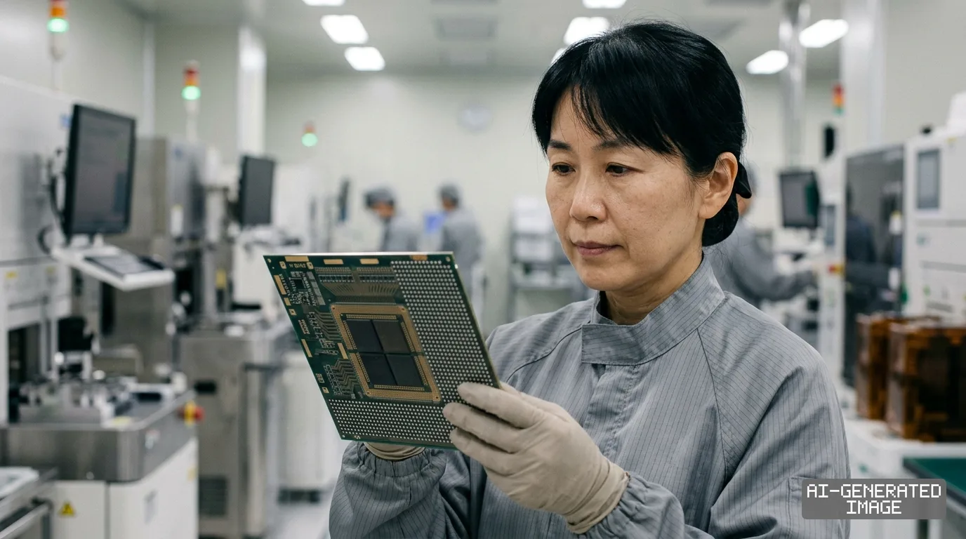
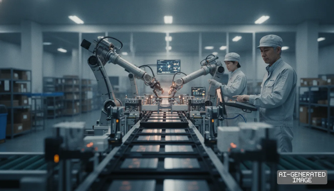
Japanese semiconductor packaging substrate manufacturers Ibiden and Shinko Electric Industries are accelerating commercial ramp schedules at their newly constructed domestic facilities to deliver high-layer flip-chip ball grid array substrates for artificial intelligence processors. The production expansions address acute supply tightness in large-body substrate panels, where multi-die accelerator designs require surface areas exceeding 10,000 square millimeters and layer counts beyond 20 build-up levels.
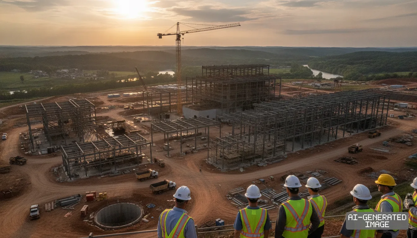
Ibiden has initiated commercial sample shipments from the second phase of its Ono Plant in Gifu Prefecture, while Shinko Electric Industries is installing panel processing tools at its new Chikuma Plant in Nagano Prefecture. The capital expenditures, committed during the initial surge in generative computing infrastructure investments, are moving into high-volume manufacturing phases as accelerator architects transition from monolithic silicon dies to multi-chiplet modules. These multi-die packaging configurations combine graphics processing units, tensor accelerators, central processing cores, and multiple stacks of high bandwidth memory on single package substrates.
For hardware procurement directors and packaging engineers at global hyperscalers, substrate surface area and layer density represent primary mechanical constraints in compute cluster deployment. A standard enterprise server processor historically required a flip-chip ball grid array (FC-BGA) substrate measuring 50 by 50 millimeters with 12 to 16 build-up layers. Advanced artificial intelligence accelerators, including modular processor systems that integrate custom application-specific integrated circuits with co-packaged optical engines and high bandwidth memory stacks, require substrate dimensions between 100 by 100 millimeters and 120 by 120 millimeters, incorporating 20 to 26 wiring layers.
The geometrical increase in panel footprint creates an exponential decrease in the net number of package units fabricated per raw panel sheet. In standard printed circuit panel processing, larger substrate dimensions lower mechanical yield due to thermal warpage during solder reflow, dielectric layer stress, and fine-line lithography distortion across broad surface areas. A defect on a single wiring layer discards the entire finished substrate unit, compounding the yield penalty on components that require more than 20 discrete lamination and microvia drilling cycles.
Ibiden remains the principal supplier of maximum-layer FC-BGA substrates to leading merchant accelerator vendors and custom silicon designers, retaining more than half of the addressable tier-one artificial intelligence server substrate market. The company has directed capital expenditure toward fine-pitch patterning lines capable of line and space design rules below 10 micrometers. Ibiden's Ono facility focuses primarily on ultra-high-density interconnect substrates that interface directly with intermediate silicon and glass interposers, supporting high-density package-on-package and multi-die topologies.
Shinko Electric Industries, an affiliated company of Fujitsu that is transitioning ownership under a consortium led by Japan Investment Corporation, is positioning its Chikuma facility to expand volume capacity for high-performance computing central processing units and custom hyperscaler server silicon. Shinko's manufacturing roadmap emphasizes micro-bump pitch scaling down to sub-50-micrometer intervals and advanced thermal dissipation core designs. The company plans to scale output incrementally throughout upcoming operational phases to serve custom compute programs contracted by North American cloud service operators.
The raw material supply chain underpinning this manufacturing expansion remains concentrated among Japanese chemical and equipment providers. High-layer FC-BGA fabrication relies almost exclusively on Ajinomoto Build-up Film (ABF), an epoxy-based insulating film manufactured by Ajinomoto Fine-Techno. The material provides the low dielectric loss and high insulation reliability required for high-frequency signal propagation between accelerator chiplets. The surge in substrate physical volume and build-up layer count has multiplied ABF consumption per finished processor package by a factor of four relative to standard server central processing units.
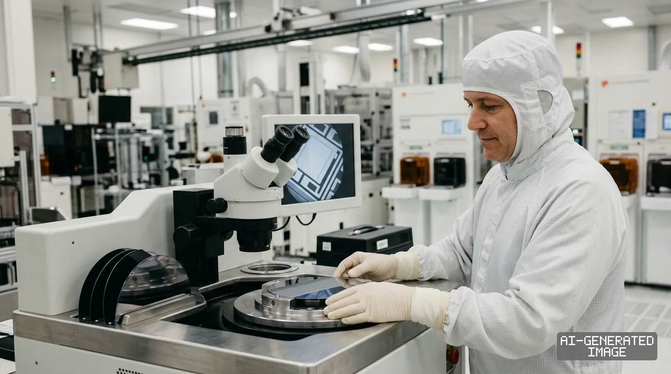
Substrate drilling and inspection capacity also dictate production velocity. The integration of 20 or more build-up layers requires hundreds of thousands of laser-drilled microvias per finished substrate panel to connect circuit traces between vertical layers. Manufacturing lines at Ibiden and Shinko rely on ultra-high-speed carbon dioxide and ultraviolet laser drilling machinery supplied by Mitsubishi Electric, alongside optical inspection and electrical testing apparatus from Japanese instrumentation specialists. The precision requirements necessary to eliminate internal voiding and trace misalignment have elongated tool qualification periods during fab setup.
Competition across the high-end packaging landscape is simultaneously prompting Taiwanese and South Korean substrate fabricators to pursue high-layer server qualifications. Unimicron Technology, Nan Ya Printed Circuit Board, and Kinsus Interconnect Technology in Taiwan, along with Samsung Electro-Mechanics and LG Innotek in South Korea, have committed substantial capital to expand their respective FC-BGA production footprints. However, tier-one accelerator designers continue to allocate the highest-complexity, maximum-area substrate designs primarily to Ibiden and Shinko due to demonstrated yield stability at layer counts exceeding 20 levels.
The delivery timetables of Ibiden's Ono lines and Shinko's Chikuma facility establish the packaging component availability baseline for high-performance server shipments through upcoming computing refresh cycles. With enterprise compute architectures shifting toward distributed chiplet architectures, substrate manufacturing yield rather than raw wafer fabrication throughput increasingly determines the net delivery schedules of finished artificial intelligence compute racks to institutional data centers.
Ibiden continues tooling qualification procedures across its Gifu operations, while Shinko Electric proceeds with customer validation testing on pilot lines at the Chikuma site.
Impact map
How this development propagates across the region and out to global buyers.
| Event | Korea | China | Japan | Global impact |
|---|---|---|---|---|
| AI Server Substrate Expansion | substrate competition intensifies | — | capacity additions at Ono and Chikuma | hyperscaler accelerator delivery timelines secured |
In this story
- Companies
- IbidenShinko Electric IndustriesAjinomotoMitsubishi Electric
- Tickers
- 4062.T6967.T2802.T6503.T
- Exposed
- Advanced Micro DevicesIntelTaiwan Semiconductor Manufacturing CompanySamsung Electro-Mechanics
- Policy
- Economic SecuritySubsidies
- Impact
- Supply ChainCapexOrder BookCost Structure
Track every Economic Security development → Track every Subsidies development →
Related briefings
- South Korean substrate makers develop embedded silicon bridges for AI chips Also on Ibiden, Shinko Electric Industries, Samsung Electro-Mechanics
- Samsung opens Yokohama chip packaging lab to rival TSMC lead Also on Ibiden, Cost Structure
- AMD raises AI accelerator prices 10% on TSMC foundry costs Also on Taiwan Semiconductor Manufacturing Company, Advanced Micro Devices, Intel
- Shinko buys Japan Display plant to build advanced packaging hub Also on Shinko Electric Industries, Cost Structure
Sources
This briefing carries no sources block. It was written from our desks’ working knowledge of the sector rather than from documents retrieved for this piece. Read it as orientation and check any figure you intend to act on — how we source briefings.
This briefing carries no linked sources: it was written from our desks' working knowledge of the sector rather than from documents retrieved for this piece. East Asia Brief publishes no citation it cannot link. Our English text is produced with AI assistance under human editorial review. See our methodology and AI policy. Spotted an error? Tell us.
The Morning Brief
What changed in Korean, Chinese and Japanese industry overnight — and what it means for your supply chain. One email, weekday mornings, US time. Free.
The Morning Brief is in preparation. Leave your address and we will write to you once — when the first issue is ready. Nothing before that.