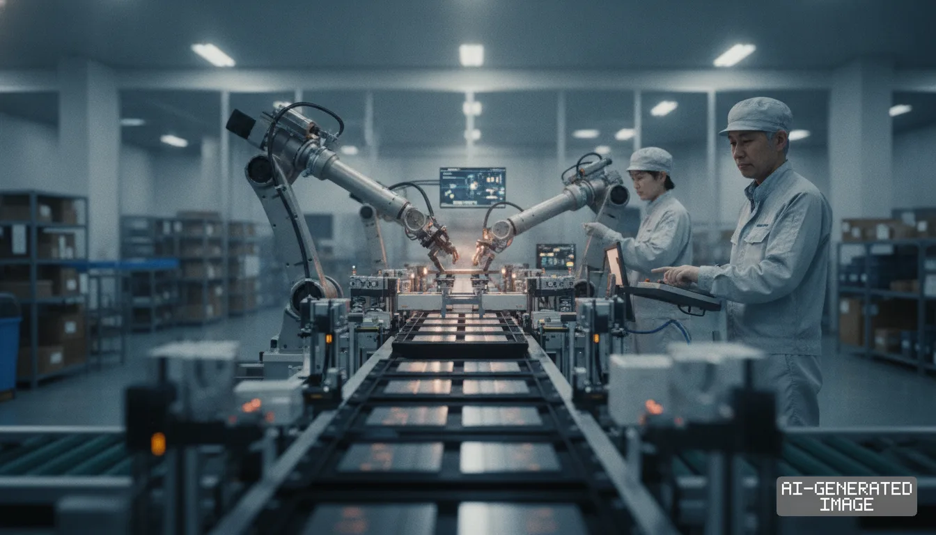
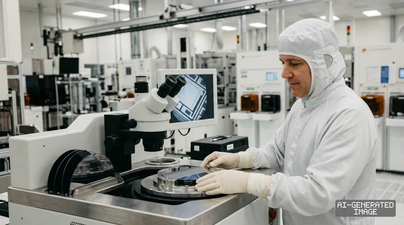
China expands 300mm silicon wafer capacity to cut reliance on Japanese suppliers
Domestic wafer manufacturers scale 12-inch polished and epitaxial shipments to supply local foundries, displacing imported substrates from Tokyo.
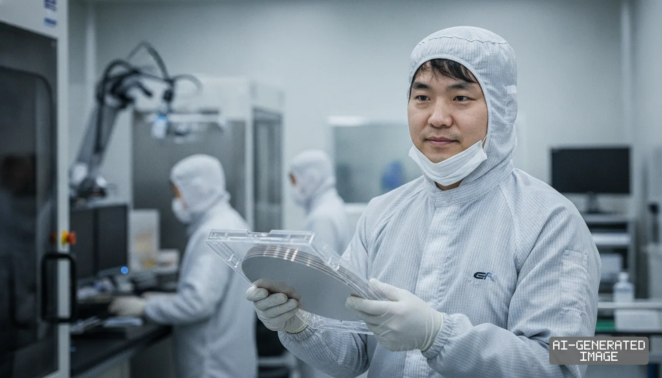
Chinese silicon wafer producers are accelerating commercial output of 300-millimeter polished and epitaxial substrates, advancing state-backed efforts to replace imports from Japanese and Taiwanese suppliers across domestic fabrication lines. Leading the buildout, National Silicon Industry Group, known as NSIG, alongside regional peers, has increased monthly 12-inch wafer capacity across facilities in Shanghai and eastern manufacturing hubs. The ramp supplies legacy and trailing-edge production nodes at Semiconductor Manufacturing International Corporation and Hua Hong Semiconductor, while initiating qualification cycles for more demanding logic and memory architectures.
The commercial scaling of 300-millimeter silicon wafers represents an operational milestone in Beijing’s strategy to insulate its semiconductor supply chain against foreign trade restrictions. Silicon wafers form the fundamental substrate for integrated circuit manufacturing, where 300-millimeter disks account for the vast majority of global volume across advanced logic, power discrete devices, and dynamic random-access memory. Historically, global supply has concentrated heavily among five dominant producers Shin-Etsu Chemical and SUMCO in Japan, GlobalWafers in Taiwan, Siltronic in Germany, and SK Siltron in South Korea which collectively command more than 85 percent of the global market. For Chinese wafer fabrication plants, reliance on these foreign vendors has created persistent vulnerability to potential export licensing controls and supply allocations.
NSIG, which operates primary 300-millimeter manufacturing through its subsidiary Shanghai Zingsemi, reported capital expenditure deployments aimed at bringing total domestic 12-inch monthly capacity beyond 600,000 wafers. Corporate regulatory disclosures filed with the Shanghai Stock Exchange show that the group’s expansion program encompasses both standard polished wafers used in power semiconductors and specialty logic, as well as thick-film and thin-film epitaxial wafers tailored for high-voltage and logic processes. Local governments in Jiangsu and Zhejiang provinces have extended infrastructure grants, power tariff offsets, and tax incentives to co-fund secondary and tertiary phases of these silicon manufacturing campuses.
For global chipmakers and materials procurement managers, the influx of domestic Chinese wafer capacity is altering regional trade flows and contract pricing structures. Domestic Chinese foundries have systematically raised local procurement quotas, prioritizing verified home-market substrate vendors over Japanese suppliers for 28-nanometer, 40-nanometer, and 55-nanometer mature production nodes. This procurement pivot has begun softening raw wafer shipment volumes into mainland China for overseas producers, who previously held near-monopoly positions across Chinese fab procurement books.
The transition, however, continues to encounter structural yield and specification differentials at advanced technology nodes. While domestic Chinese wafer makers have achieved volume parity and certified defect-density standards for trailing-edge nodes, manufacturing substrates capable of supporting sub-14-nanometer patterning, extreme ultraviolet lithography stress, and complex 3D NAND flash vertical stacking requires tighter crystalline lattice perfection and lower surface roughness. Japanese leaders such as Shin-Etsu Chemical and SUMCO retain technological moats in ultra-flat substrates, proprietary crystal growth controls, and advanced high-purity cleaning chemistries that domestic Chinese entrants are still refining through iterative customer qualifications.
Upstream raw material and tool procurement presents an ongoing operational hurdle for Chinese wafer fabricators. Manufacturing 300-millimeter ingots requires high-purity polysilicon, quartz crucibles, graphite thermal components, and high-precision diamond wire saws and chemical-mechanical planarization equipment. While domestic suppliers have localized segments of electronic-grade polysilicon and slicing tools, critical high-end crystal pullers and precision surface inspection metrology systems remain dependent on imported equipment from suppliers in Japan, the United States, and Europe. This reliance exposes secondary nodes of the substrate fabrication line to equipment export curbs and extended maintenance lead times.
Capital markets have channeled substantial state and private equity funding into midstream substrate processors through the China Integrated Circuit Industry Investment Fund, commonly designated the Big Fund. In its third financing phase, the fund allocated targeted capital injections toward wafer synthesis, advanced slicing, and defect-inspection facilities, incentivizing foundries to expand qualification pipelines for domestic materials. Fab operators that validate and integrate domestic 300-millimeter substrates receive preferential tax credits and operational subsidies under national supply chain resilience mandates, creating commercial pressure on fab managers to absorb initial yield trade-offs during process integration.
The domestic capacity additions arrive amid broader macroeconomic realignments across the international semiconductor materials landscape. As Japanese and Taiwanese wafer fabricators redirect long-term customer agreement volumes toward expansion sites in the United States, Japan, and Southeast Asia to meet capacity demands from Taiwan Semiconductor Manufacturing Company, Intel, and Samsung Electronics, Chinese substrate producers are rapidly securing residual market share within China’s expanding baseline of mature-node wafer fabs.
According to regulatory filings, NSIG's Zingsemi subsidiary is scheduled to complete equipment move-in for its latest 300-millimeter capacity module in the second half of 2026, bringing additional certified wafer lines into commercial production under existing long-term supply agreements with mainland Chinese foundries.
Impact map
How this development propagates across the region and out to global buyers.
| Event | Korea | China | Japan | Global impact |
|---|---|---|---|---|
| 300mm wafer capacity expansion | memory substrate orders shift | mature fab localization rises | raw wafer export volumes soften | substrate supply chain bifurcates |
In this story
- Companies
- National Silicon Industry GroupSemiconductor Manufacturing International CorporationHua Hong SemiconductorShin-Etsu ChemicalSUMCO
- Tickers
- 688126.SS0981.HK1347.HK4063.T3436.T
- Exposed
- GlobalWafersSiltronicSK Siltron
- Policy
- SubsidiesEconomic SecurityTax Credits
- Impact
- Supply ChainCapexPricingOrder Book
Track every Subsidies development → Track every Economic Security development → Track every Tax Credits development →
Related briefings
- SMIC narrows foundry gap with Samsung as Q2 sales surge 20% Also on Hua Hong Semiconductor, Semiconductor Manufacturing International Corporation, Pricing
- East Asia accelerates 8-inch silicon carbide capacity race as power chip makers scale output Also on SK siltron, Pricing
- Samsung Foundry converts mature planar lines to automotive power chips Also on Hua Hong Semiconductor, Pricing
- East Asian SiC wafer makers shift to laser slicing to cut 8-inch ingot processing loss Also on SK siltron
Sources
This briefing carries no sources block. It was written from our desks’ working knowledge of the sector rather than from documents retrieved for this piece. Read it as orientation and check any figure you intend to act on — how we source briefings.
This briefing carries no linked sources: it was written from our desks' working knowledge of the sector rather than from documents retrieved for this piece. East Asia Brief publishes no citation it cannot link. Our English text is produced with AI assistance under human editorial review. See our methodology and AI policy. Spotted an error? Tell us.
The Morning Brief
What changed in Korean, Chinese and Japanese industry overnight — and what it means for your supply chain. One email, weekday mornings, US time. Free.
The Morning Brief is in preparation. Leave your address and we will write to you once — when the first issue is ready. Nothing before that.