South Korean substrate makers develop embedded silicon bridges for AI chips
LG Innotek and Samsung Electro-Mechanics advance bridge-embedded FC-BGA substrates to lower 2.5D packaging costs for AI accelerators and HBM.
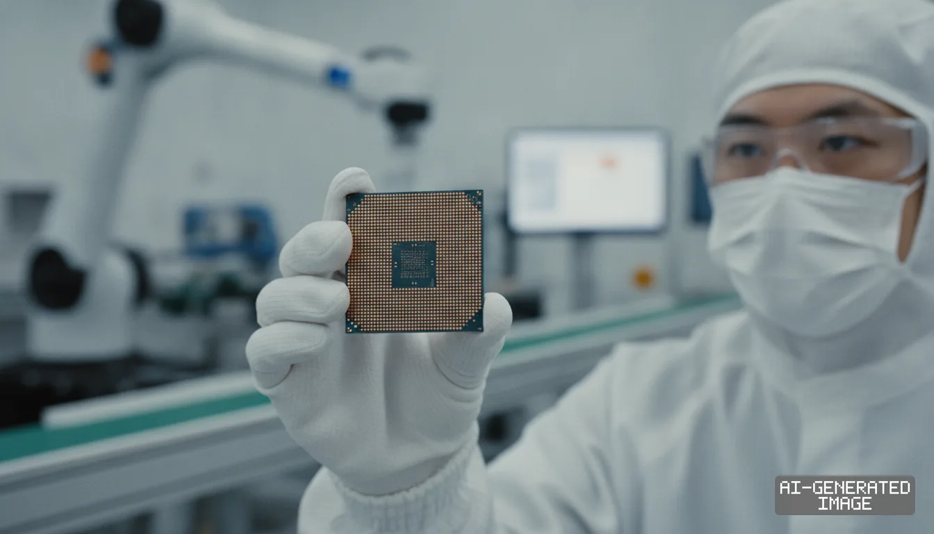
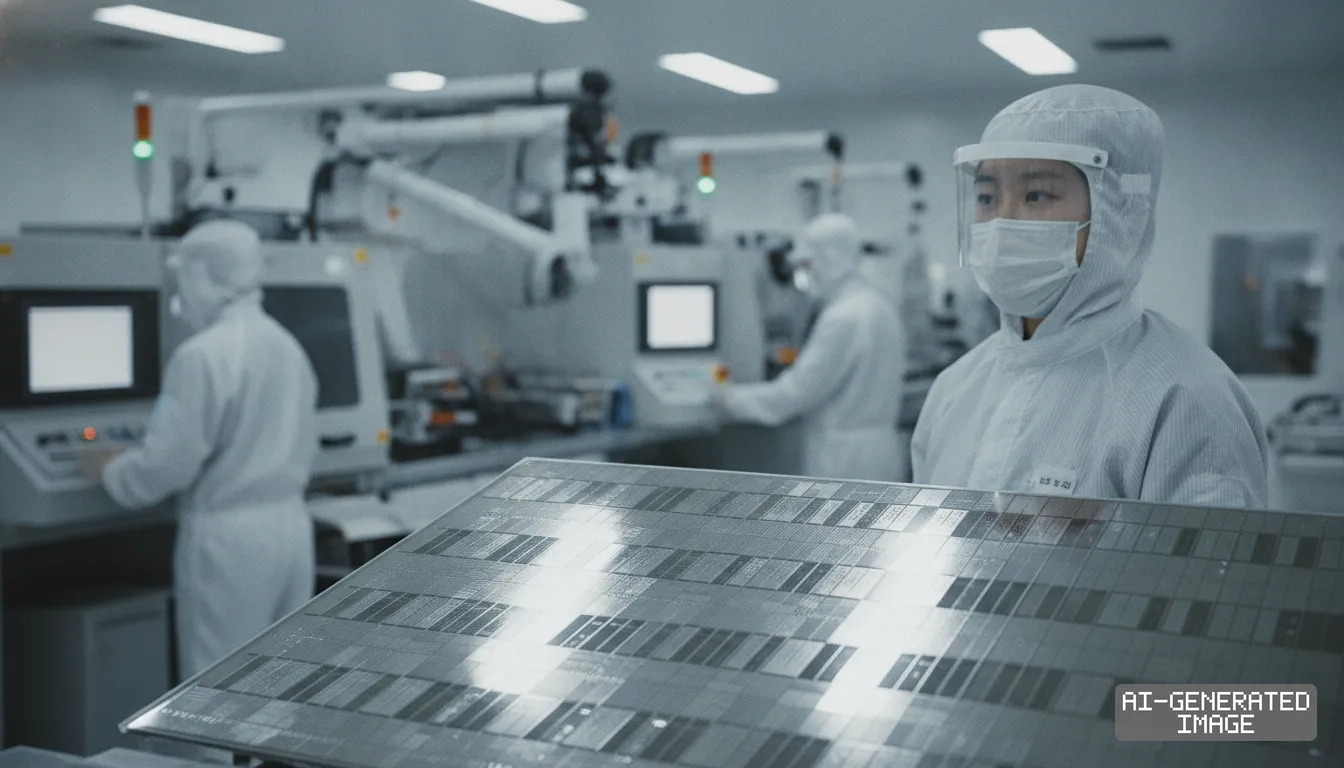
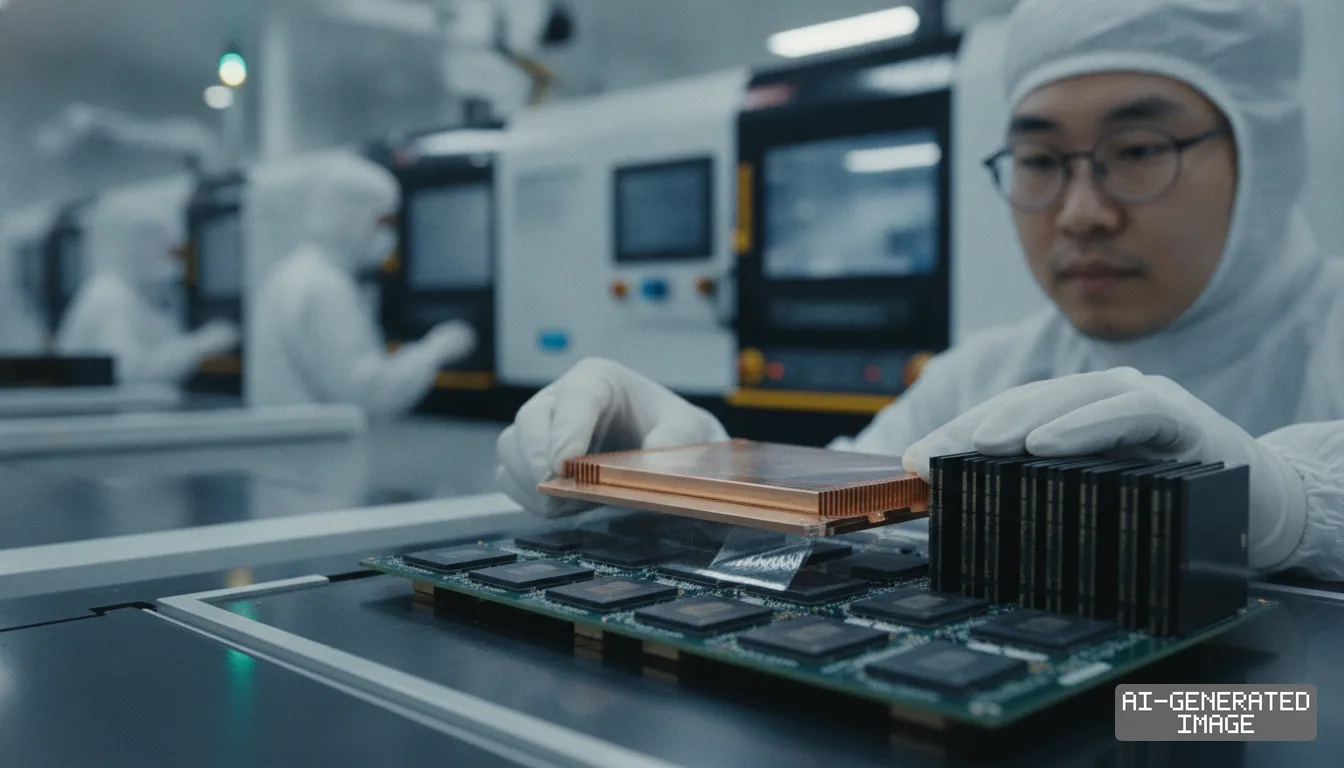
South Korean integrated circuit substrate manufacturers are developing embedded silicon bridge architectures inside organic flip-chip ball grid array (FC-BGA) substrates to meet expanding interconnect requirements for artificial intelligence accelerators and high-bandwidth memory stacks. The technological transition aims to capture packaging orders from global fabless chip designers seeking lower-cost alternatives to full-reticle silicon interposers.
Embedded silicon bridge packaging integrates micro-scale silicon routing dies directly into machined cavities within multi-layer organic substrates. This architecture replaces full-size passive silicon interposers such as those utilized in TSMC's Chip-on-Wafer-on-Substrate (CoWoS-S) by confining ultra-fine line-and-space wiring exclusively to the narrow boundary between logic computing dies and High Bandwidth Memory (HBM) modules. By localizing high-density interconnects, packaging houses reduce silicon real estate consumption, mitigate thermal stress differentials between organic and inorganic layers, and lower overall package substrate fabrication costs.
LG Innotek has stepped up development of high-density FC-BGA substrates incorporating Embedded Multi-Die Interconnect Bridge (EMIB-T) packaging techniques, designed to facilitate horizontal and vertical electrical pathways across multi-chip modules. The component maker previously supplied engineering samples of bridge-embedded organic substrates to memory manufacturer SK hynix to evaluate signal integrity and thermal dissipation performance under high-speed HBM data transfer conditions. The engineering initiative is oriented toward qualifying LG Innotek for tier-one foundry and packaging supply chains that utilize modular 2.5D bridge integration architectures.
The push into high-value semiconductor packaging follows LG Innotek's initial capital expenditure of 413 billion won ($336 million) allocated to build advanced FC-BGA manufacturing capacity at its F1 facility located in Gumi, North Gyeongsang Province. The company has expanded its manufacturing roadmaps to include bridge cavity patterning and micro-bump pitch scaling alongside standard FC-BGA production for central processing units and high-performance network processors.
Domestic competitor Samsung Electro-Mechanics is deploying a parallel structural solution under its proprietary System on Substrate (SoS) architecture. The component unit of Samsung Group manufactures server-grade FC-BGA substrates exceeding 20 internal layers, integrating embedded silicon capacitors (Si-Cap) directly beneath compute logic dies to stabilize power distribution networks during transient high-current workloads. Samsung Electro-Mechanics has directed more than 1.9 trillion won ($1.42 billion) in cumulative packaging capex toward its manufacturing hubs in Busan, Sejong, and Vietnam to refine ultra-fine wiring and warpage control processes required for large-body AI substrates.
Outsourced semiconductor assembly and test provider Amkor Technology Korea is also processing localized bridge assemblies, demonstrating fine-pitch redistribution layer (RDL) bridge packaging branded as S-Connect to bridge multi-die logic and memory in South Korea. The convergence of substrate fabrication and mid-end packaging assembly reflects structural demand shifts among AI accelerator architects, who face silicon interposer supply limits and rising substrate surface areas exceeding 100 millimeters square.
The technical barrier to commercial volume production remains formidable. Integrating rigid silicon bridges into organic substrate cores introduces yield vulnerabilities during high-temperature reflow cycles due to mismatched coefficients of thermal expansion between silicon (2.6 ppm/°C) and organic dielectric build-up films (30 to 50 ppm/°C). Precise z-axis height control inside substrate cavities is mandatory to ensure coplanarity when micro-bumps on logic and memory dies are bonded simultaneously across both the organic substrate and the embedded bridge.
The global market for bridge-embedded substrates is led by established Japanese and Taiwanese manufacturers. Ibiden and Shinko Electric Industries maintain long-standing high-volume production lines supplying Intel's EMIB packaging programs, while Unimicron Technology and Austria Technologie & Systemtechnik (AT&S) provide validated large-body substrates for server computing platforms. South Korean manufacturers entered the server-grade FC-BGA segment later than Japanese rivals, who collectively control more than half of the world's high-tier substrate capacity.
Public regulatory filings and commercial purchase orders do not yet indicate final commercial mass production sign-offs for LG Innotek or Samsung Electro-Mechanics within merchant AI accelerator lines from NVIDIA or AMD. Sourcing decisions at major fabless vendors remain tied to long-term qualification cycles, yield stabilization metrics at multi-layer thicknesses, and the assembly capabilities of designated outsourced assembly and test (OSAT) partners.
The South Korean government has designated high-density package substrates and advanced packaging integration as National Strategic Technologies under the K-Semiconductor initiative. Supervised by the Ministry of Trade, Industry and Energy (MOTIE), the policy framework provides tax credits for advanced packaging capital expenditures and funds collaborative R&D consortia linking domestic substrate makers, material suppliers, and memory fabricators across industrial clusters in Gumi, Cheonan, and Sejong.
Engineering teams at LG Innotek and Samsung Electro-Mechanics are conducting multi-physics thermal modeling, die-to-substrate co-design validations, and reliability testing on second-generation embedded bridge samples. Subsequent supplier selection stages for next-generation AI accelerator platforms will depend on certified yield data from pilot manufacturing runs scheduled throughout 2026 and 2027.
Impact map
How this development propagates across the region and out to global buyers.
| Event | Korea | China | Japan | Global impact |
|---|---|---|---|---|
| Embedded bridge substrate adoption | domestic substrate capacity expands | packaging tier excluded | market share challenged | 2.5D packaging costs drop |
In this story
- Companies
- LG InnotekSamsung Electro-MechanicsSK hynix
- Tickers
- 011070.KS009150.KS000660.KS
- Exposed
- IntelAMDAmkor TechnologyIbidenShinko Electric Industries
- Policy
- Tax CreditsSubsidies
- Impact
- Supply ChainCapexCost Structure
Track every Tax Credits development → Track every Subsidies development →
Related briefings
- Ibiden and Shinko ramp high-layer FC-BGA lines as AI server package sizes expand Also on Ibiden, Shinko Electric Industries, Samsung Electro-Mechanics
- South Korean toolmakers advance glass substrate TGV laser drillers to volume lines Also on LG Innotek, Samsung Electro-Mechanics
- Samsung opens Yokohama chip packaging lab to rival TSMC lead Also on Ibiden, Cost Structure
- Silicon interposer scaling drives foundry and OSAT shifts in 3.5D chiplets Also on Amkor Technology, Intel, Cost Structure
Sources
Reporting
Confidence: medium — how we grade this
The documents behind this briefing are linked above. East Asia Brief produces its English text with AI assistance under human editorial review, and does not translate or republish other outlets' articles. See our methodology and AI policy. Spotted an error? Tell us.
The Morning Brief
What changed in Korean, Chinese and Japanese industry overnight — and what it means for your supply chain. One email, weekday mornings, US time. Free.
The Morning Brief is in preparation. Leave your address and we will write to you once — when the first issue is ready. Nothing before that.