Foundries Standardize 300mm Silicon Photonics PDKs for AI Optical Interconnects
Commercial co-packaged optics platforms from TSMC, Samsung, and Tower target interconnect bottlenecks and thermal limits across hyperscale clusters.
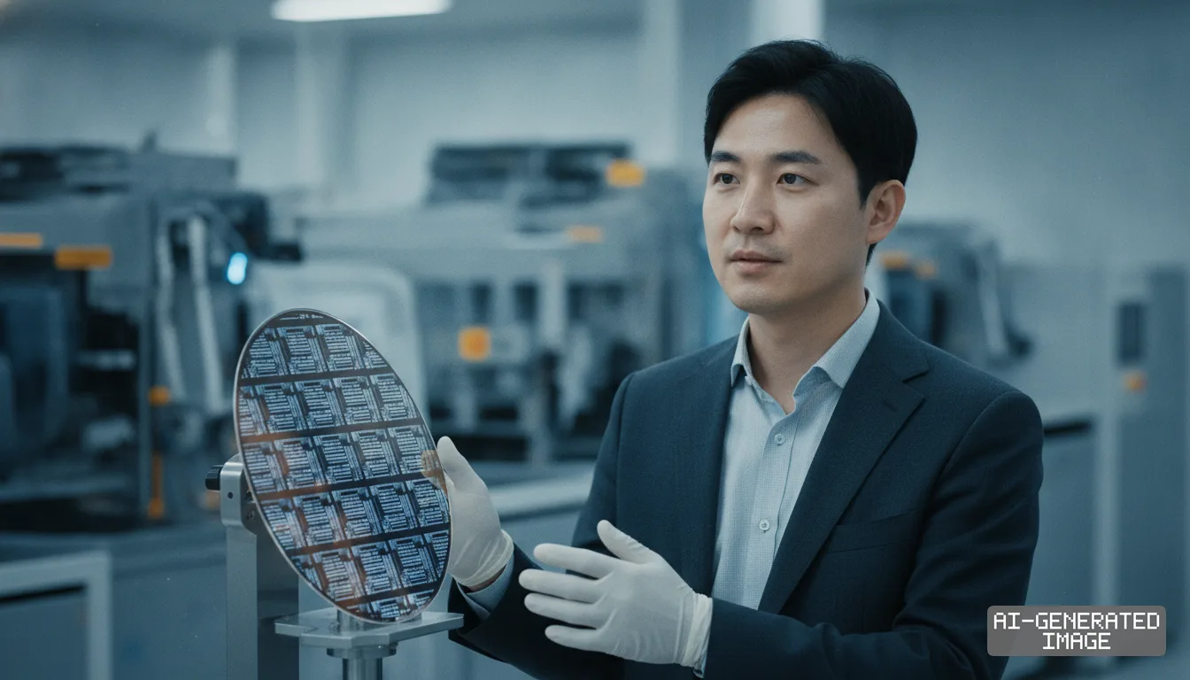
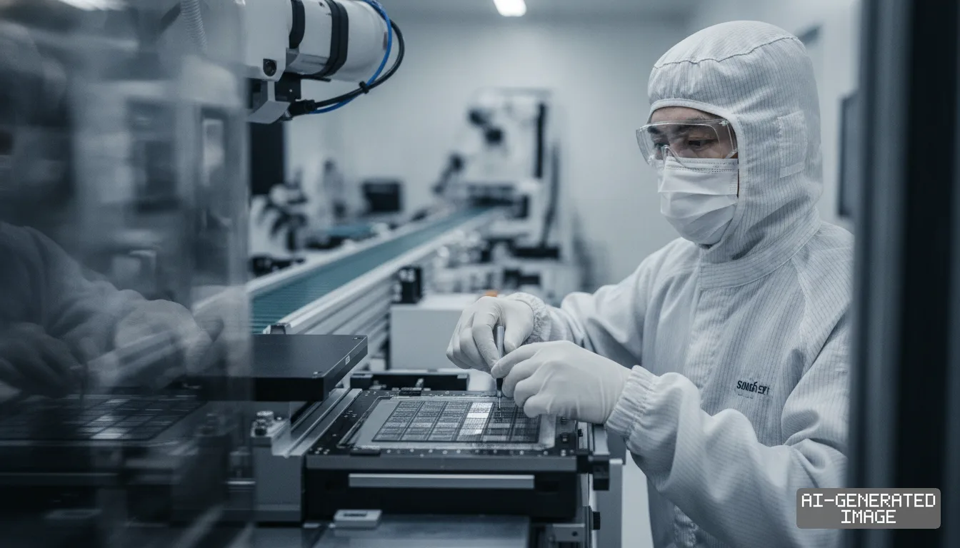
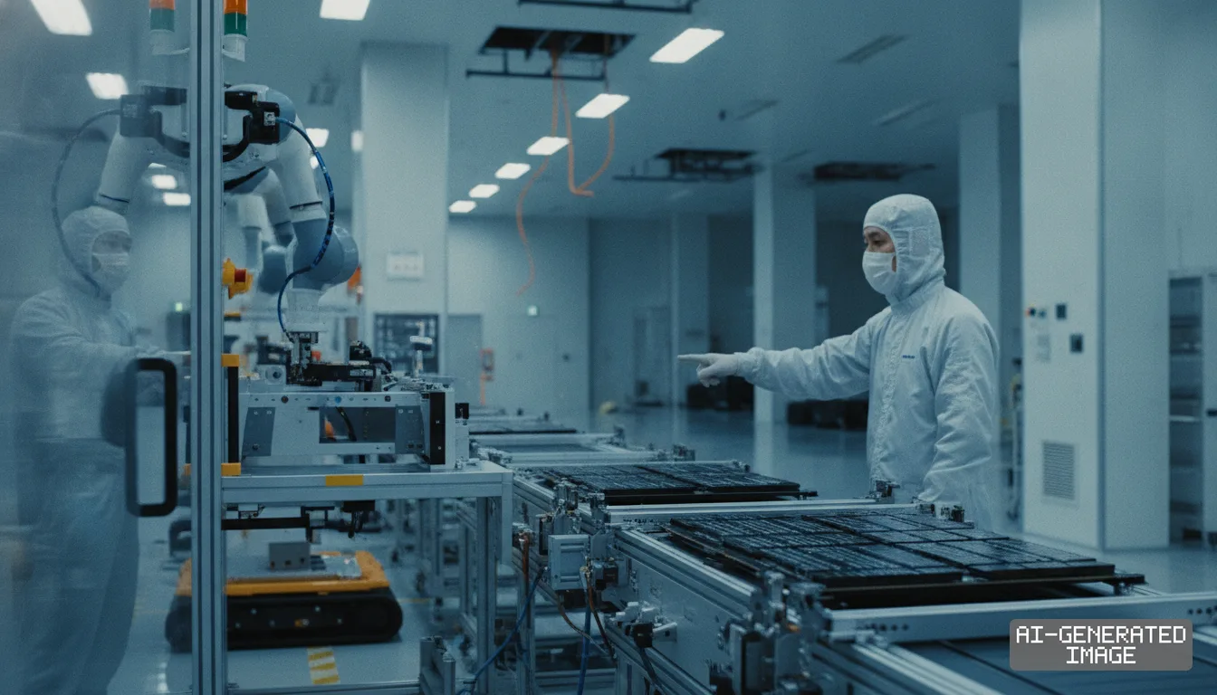
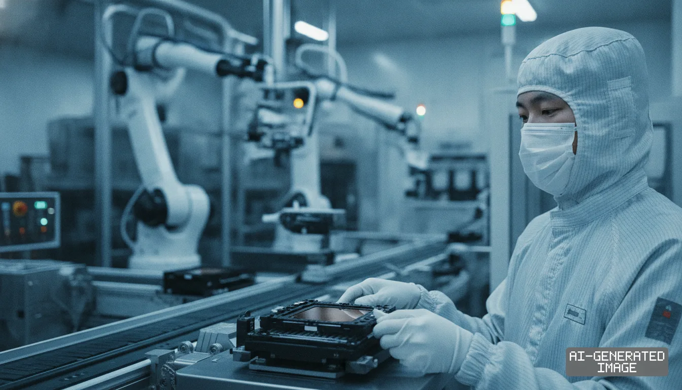
East Asian semiconductor foundries and specialty wafer fabricators are standardizing 300mm silicon photonics process design kits to support commercial co-packaged optics across hyperscale artificial intelligence clusters. The transition shifts optical interconnect manufacturing from legacy 200mm lines to standard 300mm automated complementary metal-oxide-semiconductor fabs, establishing production rules for optical waveguides, modulators, and hybrid laser integration. For system architects and hardware procurement directors, the availability of verified foundry design kits marks the threshold where optical engines move from custom lab assemblies into scalable volume components.
The architectural push stems from physical power dissipation limits in copper networking traces as cluster bandwidth scales toward 1.6 terabits per second and beyond per port. In dense accelerator racks, electrical signal attenuation across copper printed circuit board lines forces switches and network interface cards to run power-hungry digital signal processor retimers. By placing optical engines directly on the same substrate or interposer as the switch application-specific integrated circuit, co-packaged optics shortens copper traces from meters to millimeters, cutting interconnect transmission loss and system power consumption. Delivering those optical engines at data center scale requires foundries to offer standardized design rules that align photonic integrated circuits with leading-edge logic packaging.
Taiwan Semiconductor Manufacturing Company (TSMC) has established its 300mm silicon photonics roadmap around its Compact Universal Photonic Engine, designated COUPE. Officially detailed at the company's North America Technology Symposium in April 2024, the COUPE platform integrates an electronic integrated circuit die directly on top of a photonic integrated circuit die using SoIC-X three-dimensional wafer-to-wafer hybrid bonding. TSMC completed initial qualification of the engine for small form-factor pluggable modules in 2025 and is executing qualification for CoWoS advanced packaging integration to deliver monolithic co-packaged optics switches. The platform uses 300mm wafer lines to fabricate low-loss silicon and silicon nitride waveguides alongside high-speed optical modulators, minimizing die-to-die parasitic capacitance.
Industry standardization efforts in Taiwan are anchored by the SEMI Silicon Photonics Industry Alliance (SiPhIA), established in September 2024 under the joint chairmanship of TSMC and Advanced Semiconductor Engineering (ASE). On April 11, 2025, the alliance inaugurated three dedicated Special Interest Groups in Hsinchu to draft unified specifications covering optical interface tolerances, heterogeneous packaging methods, and automated wafer-level optical testing protocols. More than 110 corporate and academic members participate in the working groups, aiming to harmonize packaging form factors between fabless optical chip designers, automated testing tool vendors, and outsourced semiconductor assembly and test providers.
In South Korea, Samsung Electronics has embedded 300mm silicon photonics and co-packaged optics platforms directly within its foundry high-performance computing design infrastructure. Samsung provides fabless customers with specialized Process Design Kits (PDKs) that model passive silicon waveguides, germanium photodetectors, and thermal phase shifters within standard electronic design automation environments. The foundry platform is engineered to couple optical interconnect tiles with host logic and high-bandwidth memory stacks through Samsung's advanced two-and-a-half-dimensional packaging services, enabling customers to simulate electrical-optical domain conversions prior to tape-out.
Specialty analog and mixed-signal foundries are expanding capacity in parallel. Tower Semiconductor launched its standard 300mm silicon photonics foundry process in November 2024, providing designers with integrated silicon nitride waveguide layers, high-extinction modulators, and automated edge-coupling interfaces. In July 2026, Tower formalized a $3 billion manufacturing investment program in Japan, backed by approximately $1 billion in subsidy funding from Japan's Ministry of Economy, Trade and Industry (METI). The capital expenditure plan repurposes the Arai facility in Niigata Prefecture into an operational 300mm silicon photonics and silicon germanium production site while restructuring operations at the Uozu Fab 7 facility to expand overall 300mm wafer capacity.
A primary manufacturing hurdle facing all 300mm silicon photonics lines is wafer-level optical probe testing and yield stabilization for light sources. Unlike electrical logic wafers where automated test equipment relies on direct mechanical contact pins, photonic wafers require precision optical alignment to measure optical insertion loss, polarization dependence, and spectral response across millions of waveguide structures. Furthermore, because silicon cannot efficiently emit light due to its indirect bandgap, foundries must manage the integration of external continuous-wave laser sources or execute micro-transfer printing of indium phosphide gain chips onto the 300mm silicon base.
Despite parallel technological paths across Taiwan, South Korea, and Japan, foundry ecosystems maintain separate proprietary process parameters. While the SEMI SiPhIA framework in Taiwan addresses physical packaging interfaces and packaging interoperability, cross-foundry design portability remains restricted. A photonic integrated circuit laid out for TSMC's COUPE platform cannot be fabricated on Samsung or Tower Semiconductor 300mm lines without an extensive physical redesign of waveguide bends, grating couplers, and active modulator dopant profiles.
For procurement and hardware engineering leads, the commercialization of 300mm silicon photonics PDKs establishes clear sourcing criteria. Sourcing roadmaps must balance the higher mask costs of 300mm photonic tape-outs against the lower per-die cost, superior optical waveguide critical dimension uniformity, and advanced 3D packaging integration offered by 300mm automated fabs. The technical qualification data for next-generation switch silicon running on 300mm foundry optical engines will be reviewed during upcoming industry demonstrations scheduled for the fourth quarter of 2026.
Impact map
How this development propagates across the region and out to global buyers.
| Event | Korea | China | Japan | Global impact |
|---|---|---|---|---|
| 300mm Silicon Photonics Ramp | foundry PDK and packaging support | domestic optical transceiver testing | 300mm SiPh capacity buildout | AI cluster power reduction |
In this story
- Companies
- Taiwan Semiconductor Manufacturing CompanySamsung ElectronicsTower SemiconductorAdvanced Semiconductor Engineering
- Tickers
- 2330.TW005930.KSTSEM3711.TW
- Policy
- SubsidiesIndustrial Policy
- Impact
- Supply ChainCapexCost Structure
Track every Subsidies development → Track every Industrial Policy development →
Related briefings
- Japan optical suppliers scale laser diodes and engines for AI co-packaged optics Also on Tower Semiconductor
- IQE warns China export curbs choke indium phosphide supplies Also on Tower Semiconductor
- SK hynix and foundries advance hybrid bonding for AI silicon in 2027 Also on Taiwan Semiconductor Manufacturing Company, Samsung Electronics, Cost Structure
- Japan Expands CMP Slurry Lines for Backside Power Also on Taiwan Semiconductor Manufacturing Company, Samsung Electronics
Sources
Reporting
Confidence: medium — how we grade this
The documents behind this briefing are linked above. East Asia Brief produces its English text with AI assistance under human editorial review, and does not translate or republish other outlets' articles. See our methodology and AI policy. Spotted an error? Tell us.
The Morning Brief
What changed in Korean, Chinese and Japanese industry overnight — and what it means for your supply chain. One email, weekday mornings, US time. Free.
The Morning Brief is in preparation. Leave your address and we will write to you once — when the first issue is ready. Nothing before that.