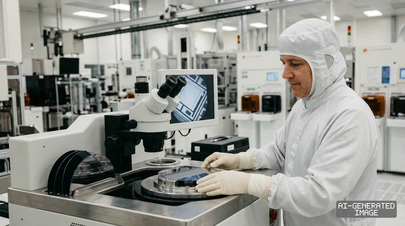
Japan mask blank makers qualify High-NA EUV substrates for sub-2nm chips
HOYA and AGC accelerate extreme low thermal expansion blank deliveries to foundries and R&D consortia as High-NA EUV lithography enters pilot production.

Japanese specialty glass and optics manufacturers HOYA Corporation and AGC Inc., together with merchant photomask manufacturer Dai Nippon Printing, have accelerated qualification runs and sample deliveries of Extreme Low Thermal Expansion mask blanks and patterned substrates to support High-Numerical Aperture extreme ultraviolet lithography lines.
Photomask blanks serve as the master templates for transferring nanometer-scale circuit blueprints onto silicon wafers. In extreme ultraviolet (EUV) lithography, light reflects off dozens of alternating molybdenum and silicon (Mo/Si) layers rather than passing through transparent quartz, making substrate surface smoothness and thermal stability critical determinants of chipmaker yield. Japanese suppliers control more than 90 percent of the commercial EUV photomask blank supply globally, creating a concentrated supply chain bottleneck for advanced semiconductor logic and DRAM manufacturing.
The transition from standard 0.33 Numerical Aperture (NA) EUV scanners to 0.55 High-NA systems alters the physical parameters of the lithography stack. High-NA scanners use anamorphic magnification, which magnifies the reticle pattern by eight times in the vertical direction and four times in the horizontal direction. This optical design cuts the exposure field size in half to 26 millimeters by 16.5 millimeters and increases the chief ray angle of incidence on the mask, worsening 3D mask topography effects such as image shadowing and pattern telecentricity errors.
To overcome these optical constraints, foundries developing 2-nanometer and sub-2-nanometer nodes require blanks with flatter low thermal expansion material (LTEM) glass substrates, surface roughness below 0.05 nanometers, and thinner absorber films. Mask blanks for High-NA tools command higher average selling prices than standard 0.33 NA EUV blanks due to tighter defect inspection criteria and specialized chemical coating steps.
HOYA Corporation has focused its development programs on next-generation mask blanks engineered for High-NA and angstrom-era nodes through bilateral testing with logic foundries. The company is qualifying low-extinction-coefficient absorber materials and phase-shift mask blank architectures that reduce mask shadowing effects while maintaining the required optical contrast. HOYA has also adjusted multilayer Mo/Si deposition parameters to minimize phase defects caused by microscopic substrate pits or bumps.
AGC Inc., operating through its subsidiary AGC Electronics in Koriyama, Fukushima Prefecture, has expanded its manufacturing footprint to supply both EUV substrate glass and coated blanks. AGC is the only manufacturer that handles the complete production sequence from raw LTEM glass melting and synthesis through surface polishing and multi-beam sputtering deposition. The company expanded EUV blank capacity at the Koriyama site by approximately 30 percent in 2025 under a capital subsidy approved by Japan's Ministry of Economy, Trade and Industry under its Program for Promoting Investment in Japan to Strengthen Supply Chains.
Merchant mask maker Dai Nippon Printing (DNP) has completed criteria evaluations for High-NA EUV photomasks and verified pattern resolution specifications for logic semiconductors beyond the 2-nanometer node. DNP began supplying evaluation photomask samples to semiconductor development consortia, equipment makers, and materials suppliers to validate lithographic performance before high-volume manufacturing. DNP is working with Japan's state-backed foundry venture Rapidus Corporation and the Interuniversity Microelectronics Centre (imec) to align mask fabrication workflows with 2-nanometer pilot operations.
Advanced foundries including Intel Foundry, Taiwan Semiconductor Manufacturing Company (TSMC), and Samsung Electronics are testing High-NA EUV reticles across pilot facilities and joint research testbeds. Intel deployed ASML's Twinscan EXE:5000 High-NA scanner at its Oregon development facility, while TSMC and Samsung have prepared mask data preparation and metrology infrastructure to evaluate High-NA insertion points for sub-2-nanometer logic nodes and advanced memory layers. Because High-NA tools cost more than $350 million per unit, foundries require zero yield-killing defects on blank substrates before exposing product wafers.
The qualification bottleneck also involves actinic mask inspection and multi-beam mask writing equipment. Japanese metrology maker Lasertec Corporation supplies actinic blank inspection and patterned mask inspection systems that use EUV wavelength light to identify sub-surface substrate defects. Pattern generation on the denser High-NA blanks relies on multibeam mask writers from NuFlare Technology and Austria-based IMS Nanofabrication, which operate at beam energies of 50 kiloelectronvolts to resolve sub-20-nanometer reticle features without overheating the chemical resist.
Commercial deliveries of production-grade High-NA EUV mask blanks are scheduled to align with foundry pilot line validation schedules through 2026, ahead of projected commercial node deployment in 2027. AGC continues commercial shipments from its Koriyama production line, while HOYA and DNP maintain active bilateral qualification cycles with leading logic chipmakers.
Impact map
How this development propagates across the region and out to global buyers.
| Event | Korea | China | Japan | Global impact |
|---|---|---|---|---|
| High-NA EUV qualification | foundry mask pilot lines | advanced node access cut off | blank makers lock in supply | sub-2nm foundry capex |
In this story
- Companies
- HOYA CorporationAGC Inc.Dai Nippon Printing
- Tickers
- 7741.T5201.T7912.T
- Exposed
- ASMLTSMCIntelSamsung ElectronicsLasertec CorporationRapidus Corporation
- Policy
- SubsidiesEconomic Security
- Impact
- Supply ChainCapexPricing
Track every Subsidies development → Track every Economic Security development →
Related briefings
- Lasertec ships EUV pellicle defect inspection tools for sub-2nm chip production Also on Lasertec Corporation
- Daifuku expands cleanroom transport backlogs as Asian chipmakers accelerate fab builds Also on Rapidus Corporation, Samsung Electronics
- Japan METI allocates clean power grid grants to anchor Hokkaido semiconductor hub Also on Rapidus Corporation
- Rapidus begins trial runs on 2nm pilot line in Hokkaido ahead of 2027 target Also on Dai Nippon Printing, ASML, TSMC
Sources
Primary documents
Reporting
Confidence: high — how we grade this
The documents behind this briefing are linked above. East Asia Brief produces its English text with AI assistance under human editorial review, and does not translate or republish other outlets' articles. See our methodology and AI policy. Spotted an error? Tell us.
The Morning Brief
What changed in Korean, Chinese and Japanese industry overnight — and what it means for your supply chain. One email, weekday mornings, US time. Free.
The Morning Brief is in preparation. Leave your address and we will write to you once — when the first issue is ready. Nothing before that.