Japan optical suppliers scale laser diodes and engines for AI co-packaged optics
Furukawa Electric and Sumitomo Electric expand continuous-wave laser output as data centers adopt external optical sources.
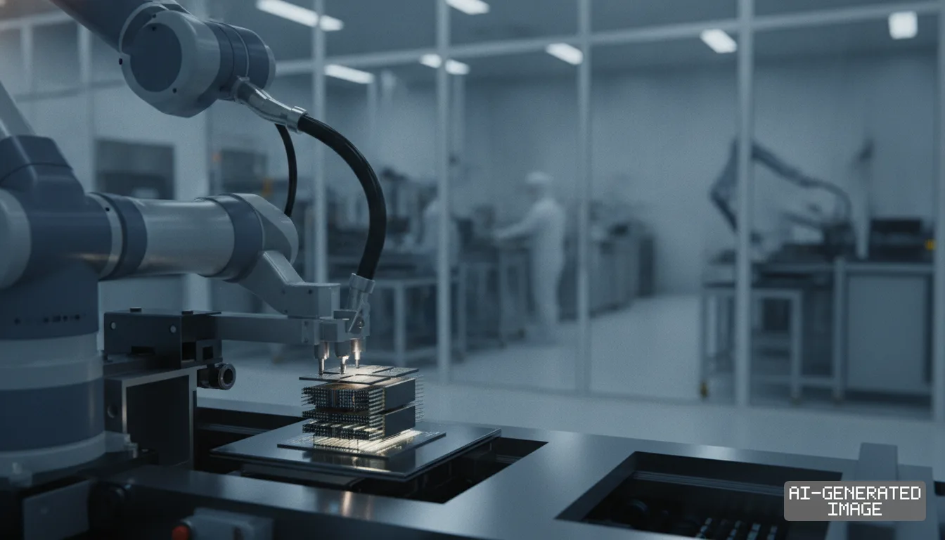
Furukawa Electric and Sumitomo Electric Industries are expanding volume production lines for high-power continuous-wave laser diodes and optical engine components, securing a critical choke point in AI hardware supply chains as hyperscale operators transition from pluggable transceivers to Co-Packaged Optics. The shift toward co-packaged architectures relocates optical engines directly onto the processor substrate alongside graphics processing units and high-bandwidth memory dies, eliminating high-frequency electrical traces to curb data transmission power loss. Because high thermal dissipation from compute silicon degrades laser diode efficiency and accelerates failure rates, data center operators are separating the light-generating element from the compute package into external laser sources that feed continuous light into silicon photonics waveguides through fiber arrays.
The transition alters procurement requirements across the physical layer of generative AI clusters. Traditional pluggable optical transceivers incorporate integrated laser diodes directly inside each module casing, distributing thermal loads across the switch faceplate. Co-Packaged Optics consolidates optical modulation onto the compute substrate, which requires continuous-wave distributed feedback lasers capable of delivering unmodulated optical power above 70 milliwatts per channel to overcome waveguide splitting and insertion losses across multi-terabit switching fabrics.
On March 27, 2024, Furukawa Electric unveiled a 16-channel blind-mate External Laser Small Form-Factor Pluggable module conforming to the Optical Internetworking Forum implementation agreement. The external laser source integrates two 8-channel transmitter optical subassemblies measuring 22.5 millimeters by 13.0 millimeters by 3.3 millimeters, supplying 100 milliwatts of optical power per channel across the 1310-nanometer wavelength band. The blind-mate mechanical interface places optical connectors on the same card-edge facet as the electrical interface inside the switch chassis, containing optical emissions within the equipment enclosure for operational safety. Furukawa began delivering engineering samples in April 2024 and scheduled commercial volume deliveries for fiscal year 2025.
Furukawa has expanded its discrete laser chip catalog to feed external light sources and silicon photonics optical engines. The company’s continuous-wave distributed feedback laser lineup includes the FOL1xQxCHP-A1 series, which delivers up to 70 milliwatts, and the FOL1xQxCHA-G1 series, which outputs 100 milliwatts per channel across four coarse wavelength division multiplexing lanes spanning 1271 nanometers to 1331 nanometers. To resolve packaging bottlenecks at the substrate boundary, Furukawa introduced a 12-fiber multi-fiber connector on March 27, 2025. The component withstands standard 260-degree Celsius surface-mount reflow soldering while occupying one-sixth the surface area of conventional multi-fiber push-on connectors, enabling direct attachment onto dense multi-chip module substrates.
In parallel, Sumitomo Electric Industries converted its continuous-wave laser diode production lines to 4-inch indium phosphide single-crystal wafers, according to an engineering report published in January 2026. The transition from legacy 2-inch and 3-inch wafer lines expands usable die output per run while improving power conversion efficiency through tighter gas-ratio and temperature controls during epitaxial crystal growth. Indium phosphide remains the sole commercially viable compound semiconductor substrate for emitting coherent light across the datacom O-band and C-band, making substrate availability a baseline requirement for continuous-wave laser production.
Sumitomo Electric expanded its upstream capacity targets to meet demand from high-speed optical module manufacturers. On July 7, 2026, the company announced an 18 billion yen ($120 million) capital expenditure plan to upgrade crystal growth and slicing lines at its Itami Works in Hyogo Prefecture. The investment raises Sumitomo Electric's planned indium phosphide substrate manufacturing capacity to 3.1 times its fiscal 2024 baseline by fiscal 2028, revising upward a November 2025 roadmap that targeted a 2.4-fold expansion. Sumitomo Electric and JX Advanced Metals supply the dominant share of high-purity semi-insulating and semiconducting indium phosphide wafers globally.
Upstream component expansion in Japan is paired with direct government funding for domestic silicon photonics foundries. On July 14, 2026, Japan’s Ministry of Economy, Trade and Industry approved a 600 billion yen ($3.7 billion) manufacturing project by Tower Semiconductor Japan under the Economic Security Promotion Act. METI committed up to 160 billion yen ($986 million) in subsidies to establish 300-millimeter silicon photonics and silicon germanium fabrication lines across facilities in Myoko, Niigata Prefecture, and Uozu, Toyama Prefecture. Under the terms of the certification, Tower Semiconductor Japan must operate the lines for at least 10 years and give priority supply to Japanese customers during market shortages.
The alignment of optical materials, laser diode fabrication, and silicon photonics foundries creates a consolidated hardware corridor for multi-terabit optical interconnects. While silicon photonics chips are processed on standard complementary metal-oxide-semiconductor foundry equipment, silicon cannot emit light efficiently due to its indirect bandgap. AI accelerator architectures designed by Nvidia, hyperscale infrastructure deployed by Microsoft, Alphabet, and Meta, and networking equipment built by Cisco Systems depend on external indium phosphide laser sources to drive silicon modulators.
Tower Semiconductor Japan is scheduled to bring equipment into its Myoko facility to begin optical chip deliveries in May 2027, followed by production startup at its new Uozu facility in the second half of 2028, as Furukawa Electric and Sumitomo Electric ramp volume shipments of laser modules and substrate materials.
Impact map
How this development propagates across the region and out to global buyers.
| Event | Korea | China | Japan | Global impact |
|---|---|---|---|---|
| AI CPO CW Laser Shift | transceiver module buyers | optical packaging firms | InP wafer and CW-LD makers | hyperscale data center clusters |
In this story
- Companies
- Furukawa ElectricSumitomo Electric IndustriesTower Semiconductor
- Tickers
- 5801.T5802.TTSEM
- Exposed
- NvidiaCisco SystemsJX Advanced Metals
- Policy
- Economic SecuritySubsidies
- Impact
- Supply ChainCapexOrder Book
Track every Economic Security development → Track every Subsidies development →
Related briefings
- TSMC signals advanced packaging backup if Intel ramp delays hit AI chips Also on Cisco Systems, Nvidia, Order Book
- Foundries Standardize 300mm Silicon Photonics PDKs for AI Optical Interconnects Also on Tower Semiconductor
- IQE warns China export curbs choke indium phosphide supplies Also on Tower Semiconductor
- TSMC weighs Texas fab campus to broaden US foundry footprint Also on Nvidia, Order Book
Sources
Primary documents
Reporting
Confidence: high — how we grade this
The documents behind this briefing are linked above. East Asia Brief produces its English text with AI assistance under human editorial review, and does not translate or republish other outlets' articles. See our methodology and AI policy. Spotted an error? Tell us.
The Morning Brief
What changed in Korean, Chinese and Japanese industry overnight — and what it means for your supply chain. One email, weekday mornings, US time. Free.
The Morning Brief is in preparation. Leave your address and we will write to you once — when the first issue is ready. Nothing before that.