Silicon interposer scaling drives foundry and OSAT shifts in 3.5D chiplets
Hybrid bonding and ultra-thin interposers reshape advanced packaging supply chains as fabless AI accelerator designers navigate front-end capacity limits.
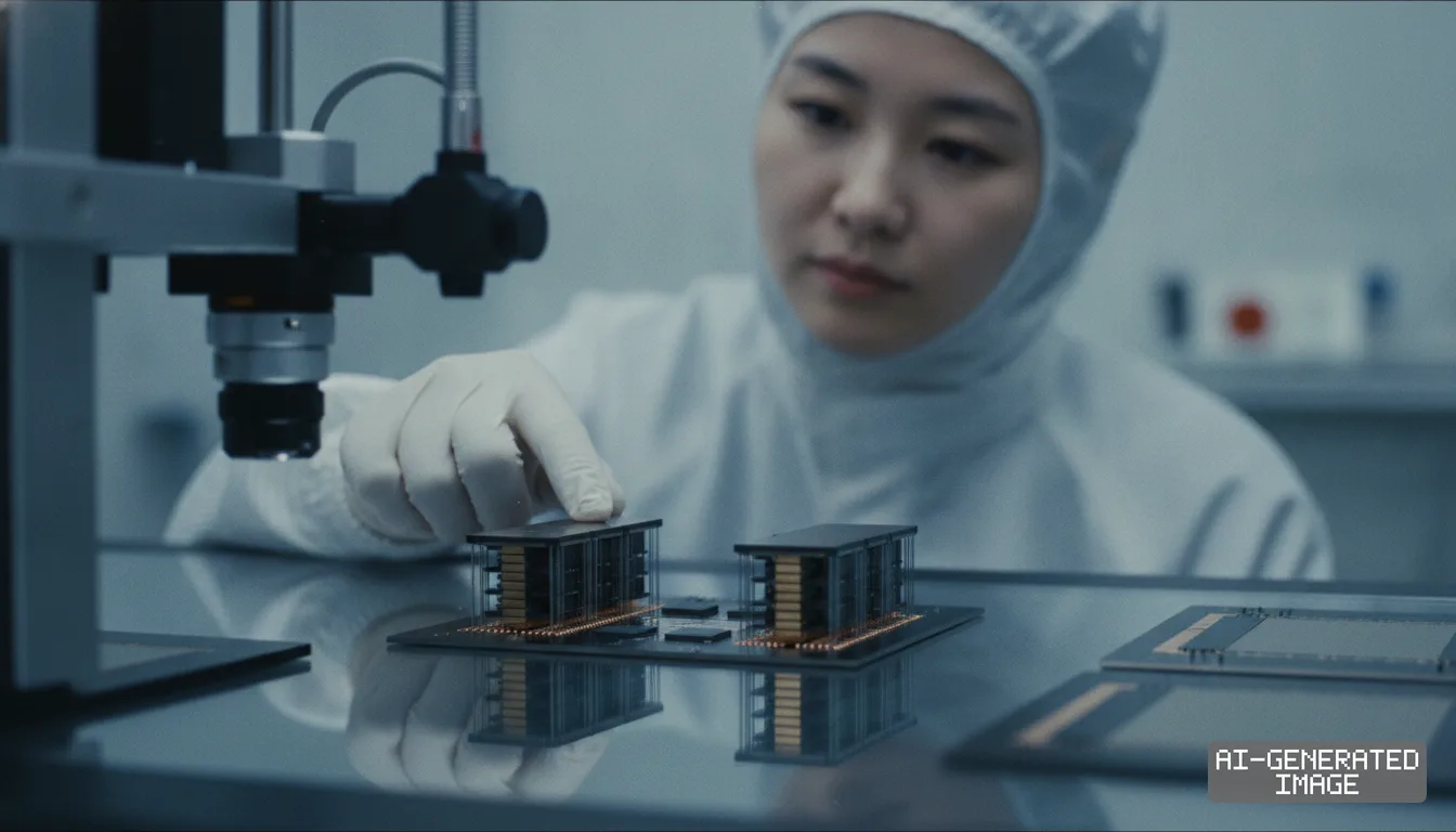
Volume deployment of 3.5-dimensional (3.5D) advanced packaging architectures is accelerating across the semiconductor sector as fabless artificial intelligence accelerator designers integrate vertical die stacking with wide-area planar interposers to bypass optical reticle limits.
The packaging architecture merges three-dimensional vertical die integration executed through direct copper-to-copper hybrid bonding or micro-bump through-silicon vias (TSVs) with two-dimensional lateral interposers, establishing high-density electrical interconnects between heterogeneous logic chiplets and High Bandwidth Memory (HBM) stacks.
Commercial demand for extreme interconnect density has concentrated production of fine-pitch silicon interposers within tier-one foundries and integrated device manufacturers (IDMs), while outsourced semiconductor assembly and test (OSAT) providers expand downstream integration capacity to ease packaging backlogs.
Broadcom demonstrated the commercial viability of multi-dimensional 3.5D integration by commencing initial customer shipments of a 2-nanometer custom compute system-on-chip built on its 3.5D eXtreme Dimension System in Package (XDSiP) platform in February 2026 for Fujitsu's MONAKA enterprise processor.
The Broadcom architecture deploys face-to-face (F2F) hybrid copper bonding to mount 2nm logic chiplets directly over 5nm SRAM cache tiles, placing the vertically integrated stacks alongside high-bandwidth memory on a CoWoS-L silicon interposer substrate scaling up to 5.5 times reticle size, or approximately 4,719 square millimeters.
Direct face-to-face copper bonding achieves a sevenfold increase in signal interconnect density and a 90 percent reduction in physical-layer interface power consumption compared to conventional planar die-to-die wiring schemes, enabling accelerator architectures to scale computational density within constrained thermal envelopes.
Advanced Micro Devices (AMD) validated the volume production of multi-tier integration in its Instinct MI300X accelerator series, which integrates 153 billion transistors across multiple compute and memory tiles by combining TSMC's System-on-Integrated-Chips (SoIC) vertical stacking at a 9-micrometer TSV pitch with a CoWoS-S silicon interposer measuring approximately 3.5 times reticle size.
In South Korea, Samsung Electronics established manufacturing baselines for wafer-thin interposer modules through its commercialized I-Cube4 heterogeneous integration platform, which places one central logic die and four HBM units on a silicon interposer thinned to approximately 100 micrometers.
Fabricating silicon interposers at thicknesses near or below 100 micrometers presents severe warpage and thermomechanical stress challenges during thermal reflow cycles, requiring specialized stress-compensation layers and mold-free structural packaging to maintain planarity across expanded surface areas.
Intel executes a modular 3.5D architecture through its EMIB 3.5D platform, integrating Foveros Direct 3D vertical stacking with Embedded Multi-die Interconnect Bridges that embed localized silicon routing bridges within organic package substrates rather than utilizing a continuous, full-reticle monolithic interposer.
The technical requirements of silicon interposer manufacturing have entrenched a structural division of labor across Northeast Asian semiconductor supply chains.
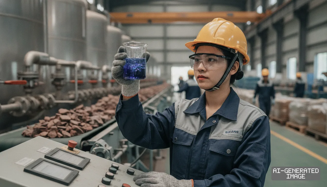
Silicon interposer fabrication relies on front-end semiconductor manufacturing processes, including deep reactive-ion etching for high-aspect-ratio TSVs, chemical-mechanical planarization, and sub-micron dual-damascene copper metallization lines, reserving primary wafer-level interposer manufacturing for front-end foundries such as TSMC and Samsung Foundry.
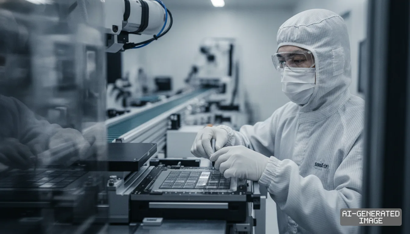
Major OSAT vendors, including ASE Technology Holding, Amkor Technology, and JCET Group, focus capital expenditure on middle-end chip-on-wafer bonding, high-pin-count substrate assembly, panel-level fan-out packaging, and system-level testing, interfacing with foundry-supplied processed interposers.
Fabless design teams continue to encounter supply-chain lead-time bottlenecks for monolithic silicon interposers exceeding three reticle sizes due to high capital intensity and mask utilization rates on advanced lithography tools at foundry facilities.
To mitigate interposer capacity constraints, packaging engineers are actively qualification-testing organic redistribution layer (RDL) interposers, glass core substrates, and embedded silicon bridge architectures that minimize overall silicon surface area consumption while sustaining necessary bandwidth metrics for next-generation generative AI clusters.
Fujitsu is scheduled to commence broader customer shipments of its 2nm MONAKA processor family utilizing Broadcom's 3.5D packaging integration in 2027 following current engineering validation trials.
Impact map
How this development propagates across the region and out to global buyers.
| Event | Korea | China | Japan | Global impact |
|---|---|---|---|---|
| 3.5D packaging scaling | foundry interposer lines | OSAT packaging assembly | MONAKA processor delivery | AI accelerator supply |
In this story
- Companies
- BroadcomTaiwan Semiconductor Manufacturing CoSamsung ElectronicsIntelFujitsuAdvanced Micro Devices
- Tickers
- AVGO2330.TW005930.KSINTC6702.TAMD
- Exposed
- ASE Technology HoldingAmkor TechnologyJCET Group
- Policy
- Economic SecuritySubsidies
- Impact
- Supply ChainCapexCost Structure
Track every Economic Security development → Track every Subsidies development →
Related briefings
- JCET expands automotive radar SiP packaging lines to capture ADAS sensor demand Also on Amkor Technology, JCET Group, ASE Technology Holding
- Foundry 2.0 Revenue Climbs 25% Also on Amkor Technology, ASE Technology Holding
- South Korean substrate makers develop embedded silicon bridges for AI chips Also on Amkor Technology, Intel, Cost Structure
- Taiwan breaks ground on TSMC packaging base to relieve CoWoS limits Also on ASE Technology Holding, Advanced Micro Devices, Taiwan Semiconductor Manufacturing Co
Sources
Reporting
Confidence: medium — how we grade this
The documents behind this briefing are linked above. East Asia Brief produces its English text with AI assistance under human editorial review, and does not translate or republish other outlets' articles. See our methodology and AI policy. Spotted an error? Tell us.
The Morning Brief
What changed in Korean, Chinese and Japanese industry overnight — and what it means for your supply chain. One email, weekday mornings, US time. Free.
The Morning Brief is in preparation. Leave your address and we will write to you once — when the first issue is ready. Nothing before that.