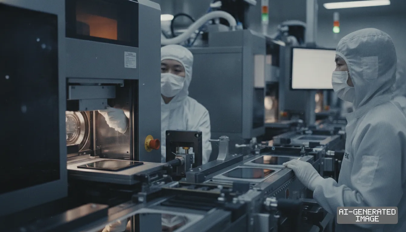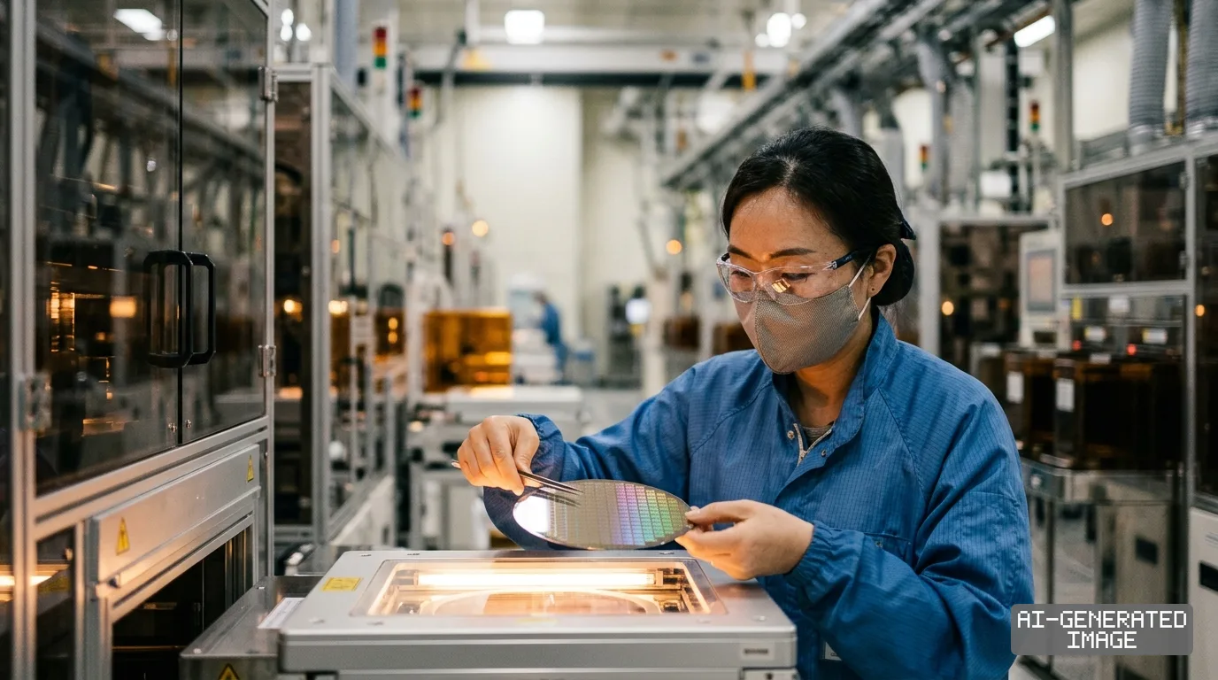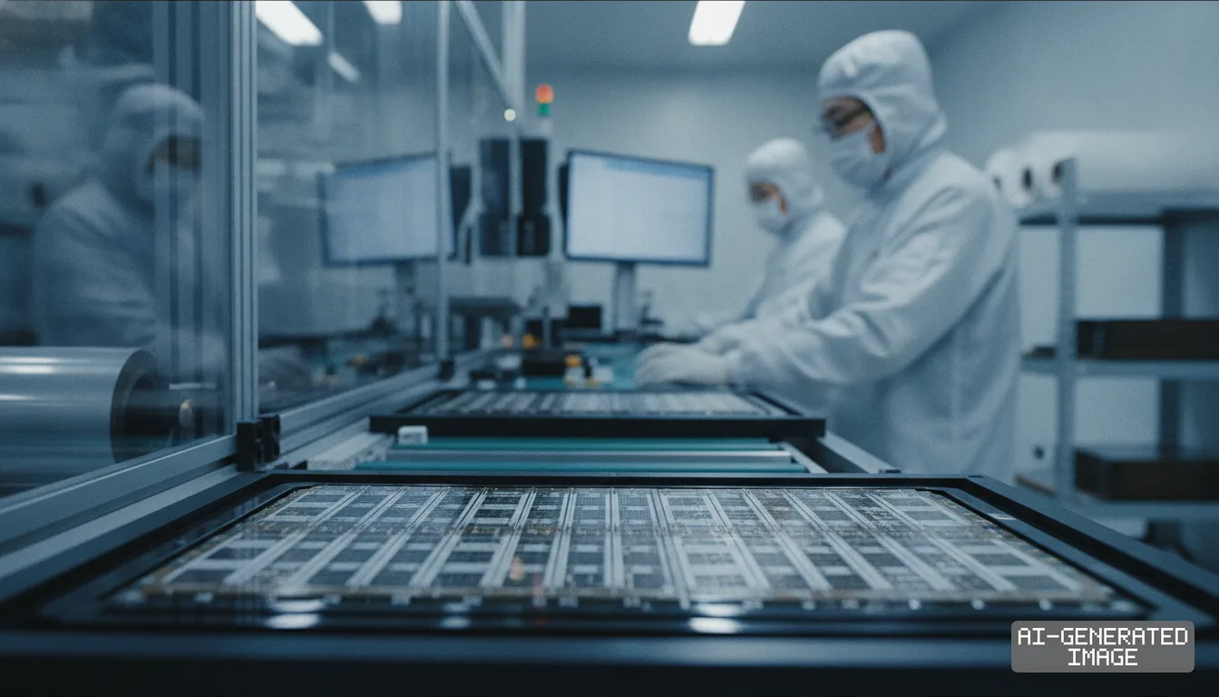
TSMC and Samsung unify 3nm base die specs for Nvidia custom HBM
Nvidia's NVHBM architecture shifts memory controllers to the base die to cut power use 15% and expand processor compute area by 25% over standard HBM4E designs.
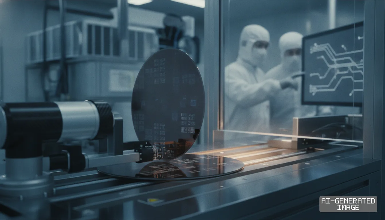
Samsung Electronics and Taiwan Semiconductor Manufacturing Co. moved Nov. 8, 2026, to coordinate production standards for custom memory base dies. The collaboration follows Nvidia's demand for uniform hardware across its artificial intelligence accelerators.
Nvidia's proprietary NVHBM specification relocates memory controllers directly into the base die. The design requires contract manufacturers to fabricate the logic platform on advanced 3-nanometer lines instead of traditional memory processes.
The custom architecture targets a 30% increase in memory bandwidth and a 15% drop in power consumption compared to standard HBM4E. It also frees up 25% of processor compute die area.
A base die sits at the bottom of a high-bandwidth memory stack. The logic slab routes data signals between vertically stacked DRAM chips and the host graphics processor.
Earlier memory generations used conventional DRAM fabrication processes to build the bottom layer. Advanced models now require leading-edge logic fabrication to manage high thermal output and fine electrical routing lines.
Samsung previously built base dies and memory core chips entirely in-house. The manufacturer produced its standard HBM4 stacks using its own 4-nanometer foundry process paired with sixth-generation 10-nanometer-class DRAM.
That integrated approach helped lift Samsung Foundry revenue during the third quarter of 2026. Executive management cited expanding base-die sales as a primary driver of improved contract manufacturing earnings.
Nvidia asked memory suppliers to unify base-die fabrication on TSMC's 3-nanometer line to ensure manufacturing consistency. SK hynix and Micron Technology received the same technical requirement.
A single foundry standard eliminates timing discrepancies across multiple suppliers during quality validation. Nvidia packages memory stacks alongside its processors using TSMC advanced packaging facilities in Taiwan.
Samsung accepted the requirement to protect its supply allocation for upcoming accelerator hardware. The decision routes the logic foundation of Samsung's memory stacks through its main contract manufacturing competitor.
Samsung will retain its proprietary 4-nanometer process for standard memory products sold to other technology customers. The company is also running internal qualification tests on its 2-nanometer lines as a secondary production option.
TSMC confirmed in April 2026 that memory base dies have become a dedicated growth sector for its 3-nanometer lines. The product group joins mobile processors and high-performance computing silicon.
The Taiwanese contract manufacturer posted third-quarter revenue of NT$1,494.24 billion ($46.7 billion). Advanced manufacturing nodes accounted for the majority of sales, running near full operational capacity.
Industry yield assessments place TSMC's mature 3-nanometer lines above 90%. Developmental 2-nanometer lines at Samsung Foundry record yields near 60%, making TSMC the lower-risk production choice for Nvidia.
SK hynix had already committed its sixth-generation base dies to TSMC under a technical partnership formed in April 2024. The supplier accounts for more than half of global high-bandwidth memory shipments.
Micron broke ground on expanded cleanrooms at its Hiroshima facility in Japan in July 2026. The manufacturer plans to combine Japanese memory dies with Taiwan-fabricated logic dies for its next accelerator products.
Standardizing the base die shifts architectural control toward the processor designer. When suppliers share an identical logic platform, memory stacks become functionally interchangeable during packaging assembly.
Interchangeable hardware limits the pricing power of individual memory makers. The arrangement allows Nvidia to adjust purchasing volumes between Samsung, SK hynix and Micron without redesigning processor interfaces.
TSMC charges roughly three to four times more for advanced logic wafers than traditional memory manufacturing costs. Hardware buyers pay the premium to remove transmission bottlenecks between memory and computing units.
Samsung is preparing expanded domestic capacity to defend its logic market share. The company plans to construct advanced manufacturing lines at its Giheung campus in South Korea costing KRW25 trillion ($18.6 billion).
Samsung also prepared its second plant in Taylor, Texas to manufacture logic base dies. The facility covers 250,000 square meters and targets commercial volume production by 2030.
That operational timeline means Samsung cannot supply domestic American base dies for near-term accelerator hardware. The delay leaves the company reliant on external contract manufacturing lines.
The three companies have not published regulatory filings or formal commercial contracts disclosing wafer supply volumes, per-unit pricing terms or a binding production schedule.
Commercial qualification tests for the custom memory base dies conclude in the first quarter of 2027, ahead of Nvidia's scheduled accelerator deployment.
Impact map
How this development propagates across the region and out to global buyers.
| Event | Korea | China | Japan | Global impact |
|---|---|---|---|---|
| Nvidia custom base die standardization | Samsung accepts external 3nm foundry routing while preserving internal 4nm lines | no domestic access to TSMC 3nm base die supply chain under export curbs | Micron Hiroshima pairs 1-beta DRAM with Taiwan logic dies | Nvidia secures multi-source interchangeability and reduces processor die area by 25% |
In this story
- Companies
- Samsung ElectronicsTaiwan Semiconductor Manufacturing Co.Nvidia
- Tickers
- 005930.KS2330.TWNVDA
- Exposed
- SK hynixMicron Technology
- Impact
- Supply ChainCapexOrder Book
Related briefings
- TSMC reviews vertical 3D DRAM production after Nvidia request Also on Taiwan Semiconductor Manufacturing Co., Micron Technology, Nvidia
- Samsung Electronics opens HBM4 base die supply to rival TSMC for AI Also on Taiwan Semiconductor Manufacturing Co., Micron Technology, Nvidia
- Micron unveils vertical HBM architecture to stack on AI GPUs Also on Taiwan Semiconductor Manufacturing Co, Micron Technology, Nvidia
- TSMC widens CoWoS supply chain with $2 billion US interposer deal Also on Taiwan Semiconductor Manufacturing Co., Nvidia, SK hynix
Sources
Primary documents
Reporting
Confidence: high — how we grade this
The documents behind this briefing are linked above. East Asia Brief produces its English text with AI assistance under human editorial review, and does not translate or republish other outlets' articles. See our methodology and AI policy. Spotted an error? Tell us.
The Morning Brief
What changed in Korean, Chinese and Japanese industry overnight — and what it means for your supply chain. One email, weekday mornings, US time. Free.
The Morning Brief is in preparation. Leave your address and we will write to you once — when the first issue is ready. Nothing before that.