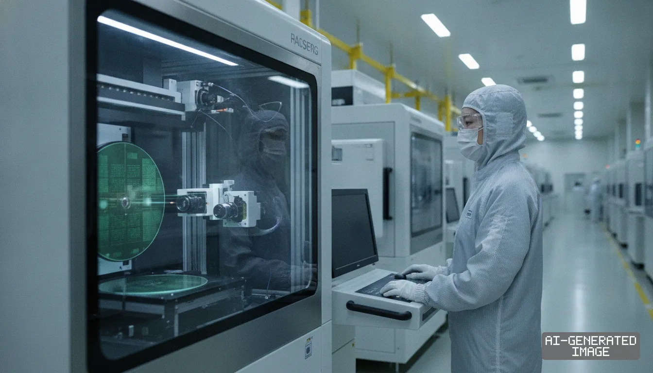
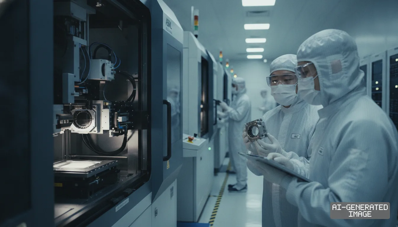
Tokyo Electron qualifies BSPDN coater-developer tracks for sub-2nm fabs
Japanese toolmakers secure process-of-record status on advanced logic pilot lines as backside power delivery doubles lithography track requirements.
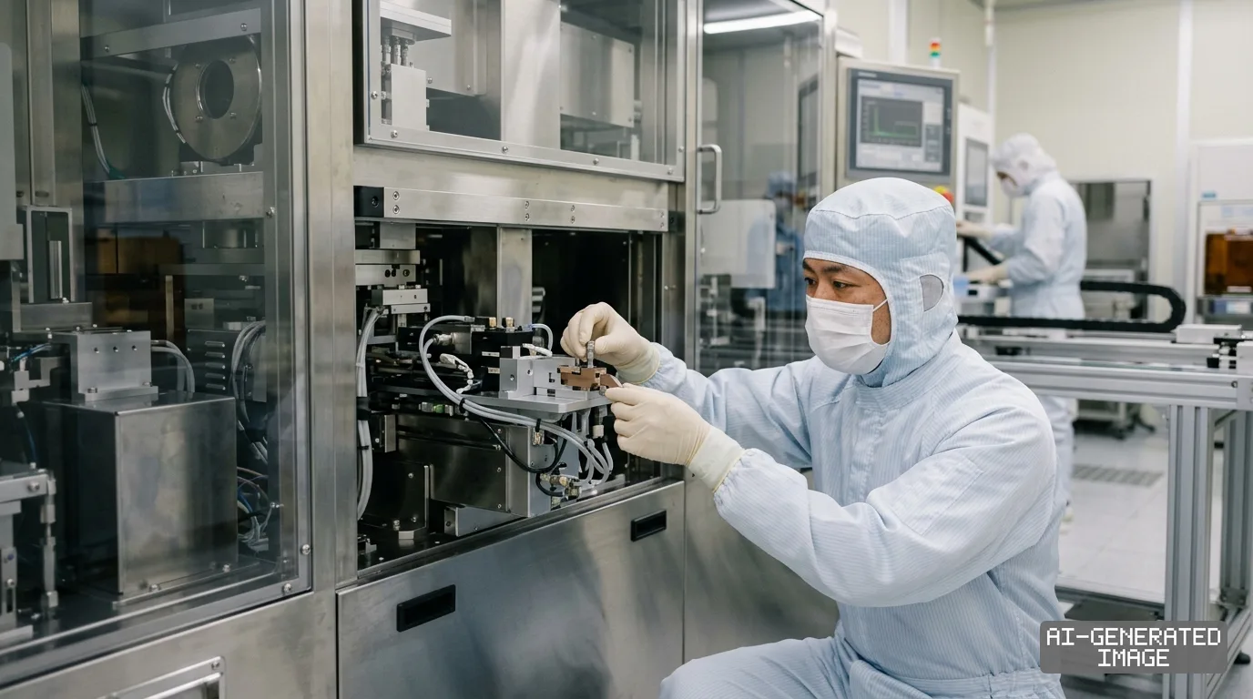
Japanese semiconductor equipment makers have secured process-of-record qualifications across advanced logic fabrication lines for specialized lithography coater-developer systems engineered to handle backside power delivery networks, locking in Japan's technological dominance over chemical dispense and wafer track processing as sub-2-nanometer node architectures approach mass production.
Tokyo Electron Limited, which commands approximately 90 percent of the worldwide photoresist coater-developer market and near-total exclusivity in High-NA extreme ultraviolet configurations, validated its CLEAN TRACK LITHIUS Pro DICE platform for advanced logic and memory transitions after introducing the 300-millimeter wafer tool in late 2025.
Backside power delivery networks, known across the industry as BSPDN, represent one of the most consequential structural design shifts in advanced semiconductor manufacturing since the introduction of FinFET transistors. By relocating power distribution rails from the frontside metal stack directly to the reverse side of the silicon substrate, chip architects decouple signal transmission from power delivery, substantially reducing resistance-capacitance delay, eliminating parasitic voltage drops, and freeing up precious frontside routing tracks for denser logic cell standard heights.
Executing this structural decoupling requires a completely new series of front-end and middle-of-line manufacturing steps that take place after the primary frontside transistor structures and interconnect layers are already formed. The device wafer must be bonded face-down to a secondary carrier wafer, mechanically ground and chemically polished to reduce the bulk silicon substrate thickness to tens of nanometers, patterned with extreme precision to reveal through-silicon power vias, and subsequently processed through multiple layers of backside metallization before debonding and final packaging.
This complex sequence places unprecedented physical stress on lithography track systems. When wafers are thinned down to sub-micrometer silicon membranes and supported solely by bonded carrier substrates, they exhibit significant mechanical warpage, asymmetric stress profiles, and localized edge distortions that disrupt conventional photoresist application. Standard spin-coating mechanisms risk generating radial thickness variations, striations, and edge-bead accumulation, which translate directly into patterning defects during extreme ultraviolet or deep ultraviolet exposure.
Because backside lithography takes place on wafers that already contain fully fabricated, high-value frontside transistors, any coating defect or yield loss at the backside stage destroys an essentially completed device. Consequently, advanced node process integration managers require coater-developer systems with extreme chemical dispense uniformity, precise wafer-edge profile control, and specialized chuck thermal management to prevent thermal expansion mismatch between the carrier substrate and the thinned device wafer during post-exposure bake cycles.
To resolve these processing hurdles, Tokyo Electron engineered the CLEAN TRACK LITHIUS Pro DICE with an updated fluidics architecture, advanced nozzle motion control, and high-precision thermal processing plates. According to technical specifications released by the company, the platform reduces wafer defectivity and associated yield loss caused by flawed photoresist coating by 50 percent or more compared to previous-generation LITHIUS Pro Z systems. The tool also increases cleanroom footprint efficiency and productivity by 25 percent or more while running the fastest coating and development sequence speeds in its product category.
Tokyo Electron confirmed in its corporate briefings for fiscal year 2026 and the first quarter of fiscal year 2027 that the LITHIUS Pro DICE platform secured Process of Record status across multiple manufacturing steps for sub-2-nanometer logic and advanced DRAM nodes. The company links its coater-developer platforms directly to its wider suite of advanced packaging and 3D integration equipment, including the Synapse series wafer bonding and debonding systems and the Ulucus series thin-wafer inspection and edge-trimming platforms, creating an integrated hardware cluster for backside processing.
Fellow Japanese equipment manufacturer SCREEN Semiconductor Solutions also maintains a presence in the track sector through its DT-3000, SOKUDO DUO, and RF-300EX platforms, addressing specialized coat and develop applications alongside advanced packaging lines. While Tokyo Electron captures the dominant share of leading-edge lithography track slots directly coupled to ASML Holding scanners, SCREEN captures significant complementary demand across BSPDN flows through its single-wafer wet cleaning and spin scrubbing platforms, which remove particulate contamination and chemical residue from thinned backsides prior to resist deposition.
The qualification of these Japanese track platforms establishes steep commercial switching barriers for competing equipment developers and reinforces the tight operational coupling between lithography scanners and coater-developer clusters. In advanced sub-2-nanometer pilot fabs, lithography coater-developers operate physically docked to EUV scanners, exchanging wafers via synchronized robotic interfaces that maintain strict environmental, chemical, and particle control.
For global semiconductor tool buyers and foundry integration teams, the deployment of specialized BSPDN track configurations drives capital expenditure intensity higher by expanding total process step counts per wafer pass. Tokyo Electron outlined in its medium-term management roadmap that the simultaneous industry transitions to sub-2-nanometer logic, Gate-All-Around nanosheets, High-NA EUV, and backside power delivery structurally expand its serviceable addressable market, increasing the number of coating, baking, developing, and cleaning cycles required across both front and back wafer surfaces.
Commercial deployment schedules show sub-2-nanometer logic nodes featuring backside power routing entering initial high-volume manufacturing lines between late 2026 and 2027, with installation of the validated LITHIUS Pro DICE tracks proceeding across leading pilot lines in Asia and North America.
Impact map
How this development propagates across the region and out to global buyers.
| Event | Korea | China | Japan | Global impact |
|---|---|---|---|---|
| BSPDN Track Qualification | foundry integration | legacy node focus | toolmaker order gains | wafer processing capex rise |
In this story
- Companies
- Tokyo ElectronSCREEN Holdings
- Tickers
- 8035.T7735.T
- Exposed
- ASML
- Policy
- Economic SecuritySubsidies
- Impact
- CapexSupply ChainOrder Book
Track every Economic Security development → Track every Subsidies development →
Related briefings
- Taiwan clears TSMC fab site for sub-1.4nm chips at Longtan Also on ASML, Tokyo Electron, Order Book
- Rapidus begins trial runs on 2nm pilot line in Hokkaido ahead of 2027 target Also on ASML, Tokyo Electron, Order Book
- Japan Linear Guide Makers Expand Ultra-Clean Units for 2nm Fab Robotics Also on ASML, Tokyo Electron, Order Book
- Comparing East Asia Fab Subsidies Across Japan, Korea, and China Also on ASML, Tokyo Electron
Sources
Reporting
Confidence: medium — how we grade this
The documents behind this briefing are linked above. East Asia Brief produces its English text with AI assistance under human editorial review, and does not translate or republish other outlets' articles. See our methodology and AI policy. Spotted an error? Tell us.
The Morning Brief
What changed in Korean, Chinese and Japanese industry overnight — and what it means for your supply chain. One email, weekday mornings, US time. Free.
The Morning Brief is in preparation. Leave your address and we will write to you once — when the first issue is ready. Nothing before that.