Samsung flags illicit etch recipe transfers to Lam Research Korea
The proprietary files cover gas chemistries and chamber settings, touching an equipment market that yielded $1.64 billion in quarterly revenue for Lam Research.
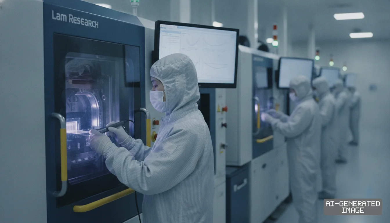
Samsung Electronics identified unauthorized transfers of advanced semiconductor etching recipes to the South Korean subsidiary of Lam Research on Nov. 9, treating the breach as a critical corporate security incident.
The disputed files contain proprietary dry-etching recipes that govern gas chemistries, chamber pressure and temperatures on advanced production lines, exceeding standard equipment maintenance agreements.
South Korea generated $1.64 billion, or 20% of Lam Research's $8.22 billion in total revenue, during the quarter ended Sept. 27, driven primarily by memory equipment deliveries.
During fiscal year 2026, South Korea generated $4.51 billion in revenue for Lam Research, accounting for 19.4% of total sales and ranking behind only China among regional markets.
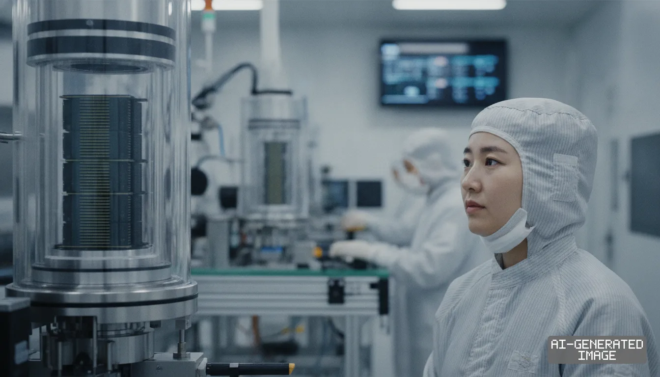
Modern semiconductor cleanrooms link production tools to internal server networks for automated monitoring. Diagnostic servers aggregate operational parameters to detect machine wear and schedule chamber maintenance before yields drop.
Wafer fabrication tool suppliers routinely collect operational telemetry to monitor hardware health and schedule parts servicing. Samsung discovered that proprietary process recipes had been bundled into unauthorized transmissions.
Process recipes specify precise chamber parameters, including radiofrequency power, process gas ratios and etching durations. Those settings determine circuit patterns on silicon wafers without causing physical defects.
Samsung uncovered the data transfers during an internal security review conducted in the second half of 2026. The probe revealed that recipe files were transferred repeatedly following improper vendor requests.
The chipmaker classified the transfers as an unauthorized leak of core intellectual property at the corporate headquarters level. The company initiated administrative controls across external technical support channels.
Lam Research Korea announced a chief executive change on Nov. 6, replacing Park Joon-hong with Kim Tae-won. Park had served as regional president for two years and nine months.
Kim previously led process engineering and product deployment in the etch business unit at Lam Research headquarters in Fremont, California. He relocated to Yongin, South Korea, to lead operations.
Lam Research supplies specialized dry-etching equipment to Samsung production sites in Pyeongtaek and Hwaseong. The Korean chipmaker accounts for a primary share of the supplier's installed wafer equipment base.
Dry etching uses chemical plasma to carve microscopic patterns into silicon wafers. In high-density flash memory and advanced DRAM, etching tools must drill deep microscopic holes through hundreds of stacked layers.
Developing viable etch recipes requires years of iterative adjustments to protect wafer uniformity. Chip fabricators consider custom recipes proprietary trade secrets distinct from the machinery hardware specifications.
Commercial contracts between fabricators and tool vendors define boundaries for remote equipment diagnostics. Service agreements permit sensor telemetry collection while prohibiting extraction of client process sequences.
The incident highlights compliance challenges when equipment manufacturers service multiple competing fabrication accounts. Leading semiconductor makers enforce strict isolation protocols to prevent data migration between customer programs.
South Korea designates advanced memory design and fabrication technologies as national core assets under technology protection laws. The statutes impose strict disclosure limits on proprietary semiconductor manufacturing techniques.
The South Korean government has not published an official investigation notice, and authorities have not announced formal charges against any corporate entity or personnel.
Lam Research has not disclosed any regulatory inquiry or pending litigation related to the matter in filings with the U.S. Securities and Exchange Commission.
Samsung has not published an estimate of financial damage resulting from the data transfers, nor has it filed a public criminal complaint.
Global memory production relies heavily on a small group of specialized equipment vendors. Lam Research, Applied Materials and Tokyo Electron control the vast majority of advanced etch and deposition systems.
Switching equipment suppliers at operating fabrication plants requires extensive qualification cycles and substantial capital expenditures. Samsung continues regular manufacturing operations while adjusting data transmission procedures.
Kim assumed executive duties at the Korean subsidiary following the Nov. 6 leadership change, while Samsung prepares updated data compliance guidelines ahead of vendor reviews in the first quarter of 2027.
Samsung maintains routine fab operations and tool servicing at its fabrication facilities as internal data security audits continue.
Impact map
How this development propagates across the region and out to global buyers.
| Event | Korea | China | Japan | Global impact |
|---|---|---|---|---|
| Etch recipe data breach probe | Samsung tightens cleanroom telemetry access across memory lines | Domestic memory fabs maintain strict vendor access controls | Tokyo Electron audits service team data collection protocols | Leading chipmakers reinforce supplier network barriers to guard IP |
| Etch recipe data breach probe | Samsung tightens cleanroom telemetry access across memory lines | Domestic memory fabs maintain strict vendor access controls | Tokyo Electron audits service team data collection protocols | Leading chipmakers reinforce supplier network barriers to guard IP |
In this story
- Companies
- Samsung ElectronicsLam Research
- Tickers
- 005930.KSLRCX
- Impact
- ComplianceSupply Chain
Related briefings
- Korea opens US talks as tool license delays hit SK hynix Dalian Also on Lam Research, Samsung Electronics, Compliance
- SK hynix seeks US export clearance for Wuxi memory equipment Also on Lam Research, Samsung Electronics, Compliance
- Samsung denies Chinese tool testing as US tightens fab controls Also on Lam Research, Samsung Electronics, Compliance
- Samsung and SK hynix upgrade China memory fabs to 286 layers Also on Lam Research, Samsung Electronics
Sources
Primary documents
Reporting
Confidence: high — how we grade this
The documents behind this briefing are linked above. East Asia Brief produces its English text with AI assistance under human editorial review, and does not translate or republish other outlets' articles. See our methodology and AI policy. Spotted an error? Tell us.
The Morning Brief
What changed in Korean, Chinese and Japanese industry overnight — and what it means for your supply chain. One email, weekday mornings, US time. Free.
The Morning Brief is in preparation. Leave your address and we will write to you once — when the first issue is ready. Nothing before that.