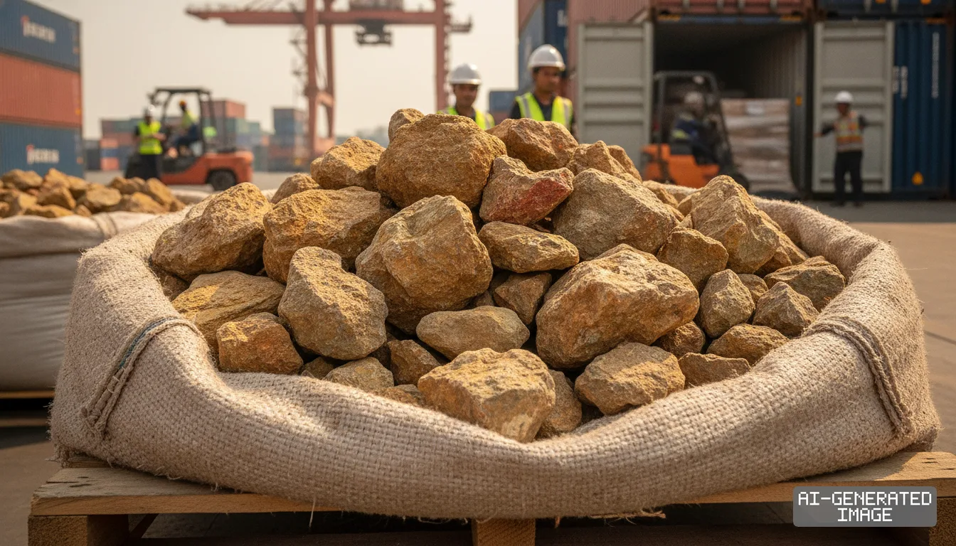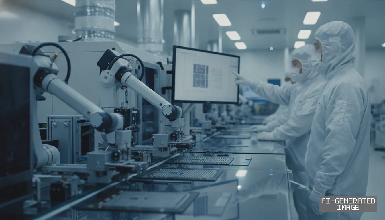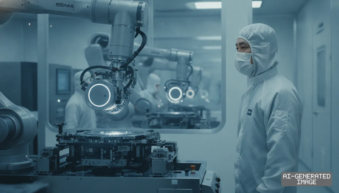
Applied Materials opens $5B EPIC hub to Korean memory makers
Samsung Electronics and SK hynix will run joint cleanroom trials inside the 600,000-square-foot California complex to cut development cycles for HBM4 and sub-10-nanometer memory.
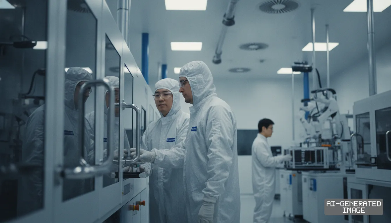
Applied Materials advanced operational cleanroom access at its $5 billion EPIC Center on Oct. 22, 2026, pairing engineers with founding partners Samsung Electronics and SK hynix to accelerate next-generation memory production.
The Sunnyvale, California, complex spans 600,000 square feet and houses nearly four acres of advanced cleanroom space. The $5 billion capital expenditure marks the largest private investment in collaborative semiconductor manufacturing equipment research.
Samsung Electronics and SK hynix together supply more than 70% of global dynamic random-access memory and over 90% of high-bandwidth memory. Both manufacturers face physical scaling barriers as dynamic random-access memory (DRAM) circuitry approaches the 10-nanometer threshold.
The collaborative center alters how production machinery and process chemistries are engineered. Instead of developing equipment in isolation before shipping test tools overseas, toolmakers and device manufacturers work inside shared cleanroom bays.
The parallel workflow shortens technology development cycles by several quarters, the equipment vendor said. Engineers can validate atomic-level deposition, etching and chemical mechanical planarization directly on commercial 300-millimeter silicon wafers.
Chemical mechanical planarization — an abrasive polishing step that levels wafer topography — becomes critical as memory dies stack higher. Planar surfaces prevent structural defects when connecting vertical interconnects through multiple silicon layers.
Samsung Electronics joined the facility as a founding partner in February, while SK hynix finalized its partnership agreement in March. Both Korean chipmakers are preparing high-volume production for sixth-generation high-bandwidth memory, designated as HBM4.
HBM4 stacks 16 DRAM dies vertically on top of an advanced logic base die. The design requires hybrid bonding and extreme ultraviolet lithography steps that demand atomic-scale placement precision.
Applied Materials supplies critical systems for atomic layer deposition, selective epitaxy and advanced packaging. Epitaxy systems deposit crystalline layers atom by atom, altering electrical conductivity without increasing physical transistor dimensions.
The company's new selective epitaxy system increases DRAM transistor performance while reducing cleanroom footprint by 20%, according to investor disclosures. Those efficiency gains permit memory producers to expand output within existing building shells.
Advanced logic foundry leader TSMC, Intel and Micron Technology round out the founding partner cohort. Toolmaker Screen Semiconductor Solutions and test equipment supplier Advantest participate as innovation partners alongside Japanese memory producer Kioxia and Dutch hybrid bonding specialist Besi.
SK hynix supplies more than 50% of the world's commercial HBM3E modules, primarily delivering components for Nvidia artificial intelligence accelerators. The Icheon-based memory maker plans to deploy custom logic base dies fabricated by TSMC for its upcoming HBM4 architecture.
Samsung Electronics operates both foundry and memory fabrication divisions, controlling roughly 40% of global DRAM wafer processing capacity. The company is developing proprietary DRAM architectures to secure volume orders for enterprise artificial intelligence server clusters.
The shared Silicon Valley facility allows Korean process engineers to evaluate new machine configurations months before high-volume tools ship to Pyeongtaek or Icheon. Early cleanroom optimization prevents yield loss during initial fab installations.
The transition toward three-dimensional DRAM architectures forces radical changes in materials science. Conventional cylindrical capacitor structures struggle to store sufficient electrical charge when cell critical dimensions drop below 11 nanometers.
Memory manufacturers are evaluating ruthenium and molybdenum metal lines to replace conventional tungsten, which exhibits elevated electrical resistance at narrow dimensions. Applied Materials develops the selective deposition chambers required to handle those metals.
Applied Materials raised its planned capital commitment for the EPIC Center from an initial $4 billion announced in May 2023 to $5 billion. The adjustment reflects increased customer demand for specialized advanced packaging and transistor scaling chambers.
The foundation of the Sunnyvale facility required enough concrete to fill 34 Olympic-sized swimming pools. The structure incorporates enough steel reinforcement to match the weight of two Eiffel Towers, supported by 34 cleanroom roof trusses.
Applied Materials will report its fourth-quarter and fiscal 2026 financial results on Nov. 12, 2026. Executive management will review initial operational progress and customer co-development activity during the scheduled conference call.
Published notices by Applied Materials on Oct. 22 do not establish a new legal partnership filing, as formal founding agreements with Samsung Electronics and SK hynix took effect earlier in 2026. The vendor has not published specific capital allocations contributed by individual partners.
Cleanroom qualification workflows completed in California will transfer to customer volume production lines ahead of scheduled commercial ramps in 2027.
Impact map
How this development propagates across the region and out to global buyers.
| Event | Korea | China | Japan | Global impact |
|---|---|---|---|---|
| EPIC Center cleanroom integration | Samsung and SK hynix shorten HBM4 validation cycles ahead of 2027 mass production | CXMT remains excluded from advanced US co-development platform | Screen and Kioxia access joint development for next-generation etch and NAND | AI memory packaging roadmap accelerates yield improvements across sub-10nm DRAM |
In this story
- Companies
- Applied MaterialsSamsung ElectronicsSK hynix
- Tickers
- AMAT005930.KS000660.KS
- Exposed
- TSMCMicron TechnologyIntel
- Impact
- CapexSupply Chain
Related briefings
- Intel joins Applied Materials in $5 billion chip R&D hub Also on Applied Materials, Intel, Micron Technology
- Taiwan clears TSMC fab site for sub-1.4nm chips at Longtan Also on Applied Materials, Intel, TSMC
- SK hynix and foundries advance hybrid bonding for AI silicon in 2027 Also on Applied Materials, Intel, SK hynix
- SK hynix seeks US export clearance for Wuxi memory equipment Also on Applied Materials, Micron Technology, SK hynix
Sources
Primary documents
Reporting
Confidence: high — how we grade this
The documents behind this briefing are linked above. East Asia Brief produces its English text with AI assistance under human editorial review, and does not translate or republish other outlets' articles. See our methodology and AI policy. Spotted an error? Tell us.
The Morning Brief
What changed in Korean, Chinese and Japanese industry overnight — and what it means for your supply chain. One email, weekday mornings, US time. Free.
The Morning Brief is in preparation. Leave your address and we will write to you once — when the first issue is ready. Nothing before that.