Intel joins Applied Materials in $5 billion chip R&D hub
The partnership connects Oregon labs to Silicon Valley cleanrooms as foundry rivals TSMC and Samsung Electronics share toolmaker research space to curb node costs.
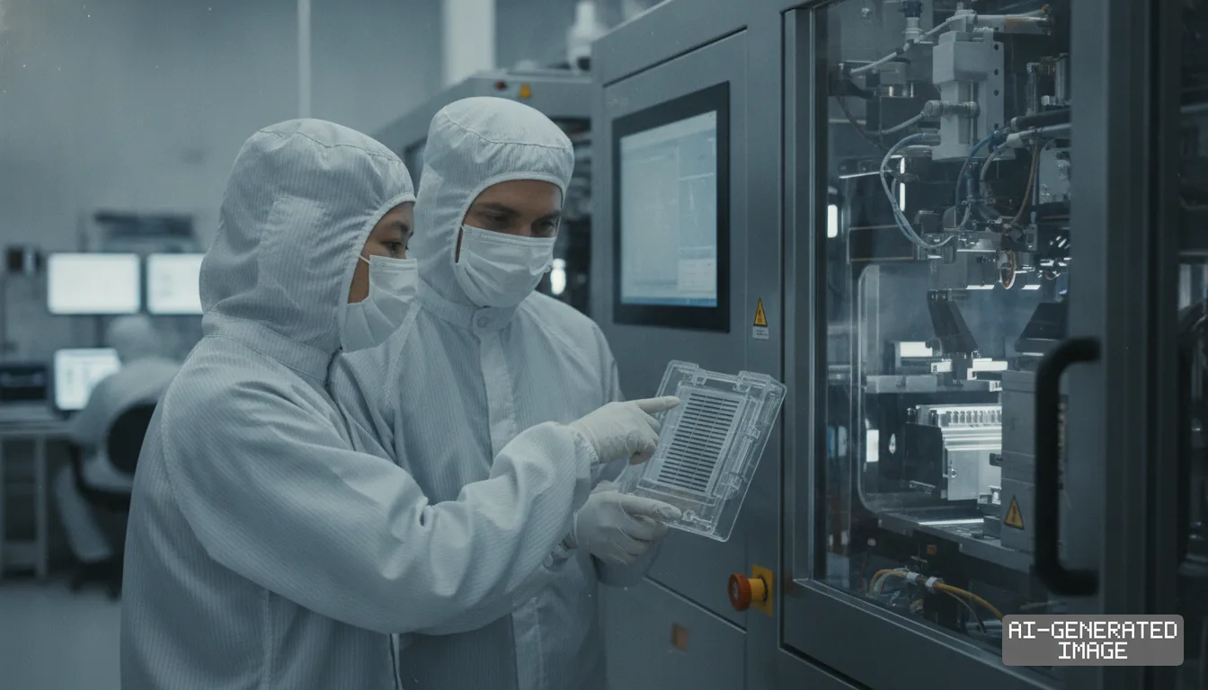
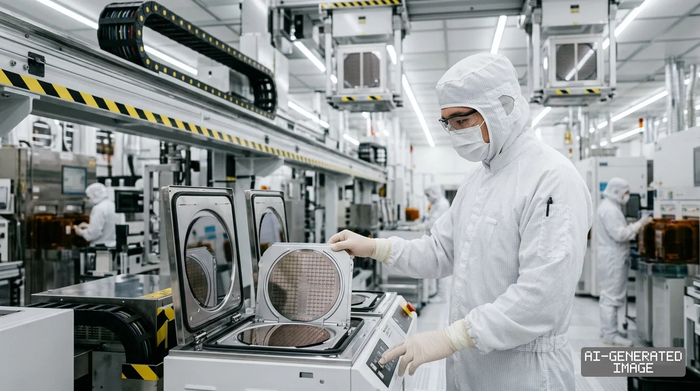
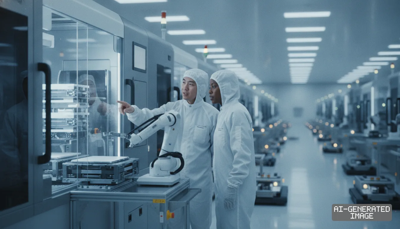
Intel joined Applied Materials' $5 billion semiconductor research facility on Oct. 8, 2026, partnering with the toolmaker to accelerate advanced transistor architecture, power delivery interconnects and Foveros three-dimensional packaging for artificial intelligence processors.
The joint effort connects Intel's primary technology development campus in Hillsboro, Oregon, with the Equipment and Process Innovation and Commercialization Center, or EPIC Center, located in Sunnyvale, California.
The documents behind this briefing are linked above. East Asia Brief produces its English text with AI assistance under human editorial review, and does not translate or republish other outlets' articles. See our methodology and AI policy. Spotted an error? Tell us.