Taiwan clears TSMC fab site for sub-1.4nm chips at Longtan
The National Development Council approved an NT$95.6 billion layout across 104 hectares, granting Taiwan Semiconductor Manufacturing Co. ground for three facilities after 2028 reviews.
Taiwan's National Development Council approved on Sept. 18, 2026, an expanded science park proposal in Longtan, clearing land for TSMC to construct sub-1.4-nanometer chip fabrication facilities.
The decision clears administrative hurdles for the Longtan Phase 3 project in Taoyuan. The site serves as the domestic hub for semiconductors beyond the 1.4-nanometer generation, the agency said.
Development costs for the baseline park infrastructure will reach NT$95.63 billion ($3.0 billion). The state-backed budget finances site preparation, utility links and transport access for incoming tenants.
The approved parcel spans 104.19 hectares, with roughly 46 hectares designated strictly for industrial production. That footprint is smaller than the original 158.59-hectare design drafted in 2023.
Planners reduced the boundary by more than a third to ease community disputes over land acquisition. Residential protests had stalled the earlier expansion three years ago, the council said.
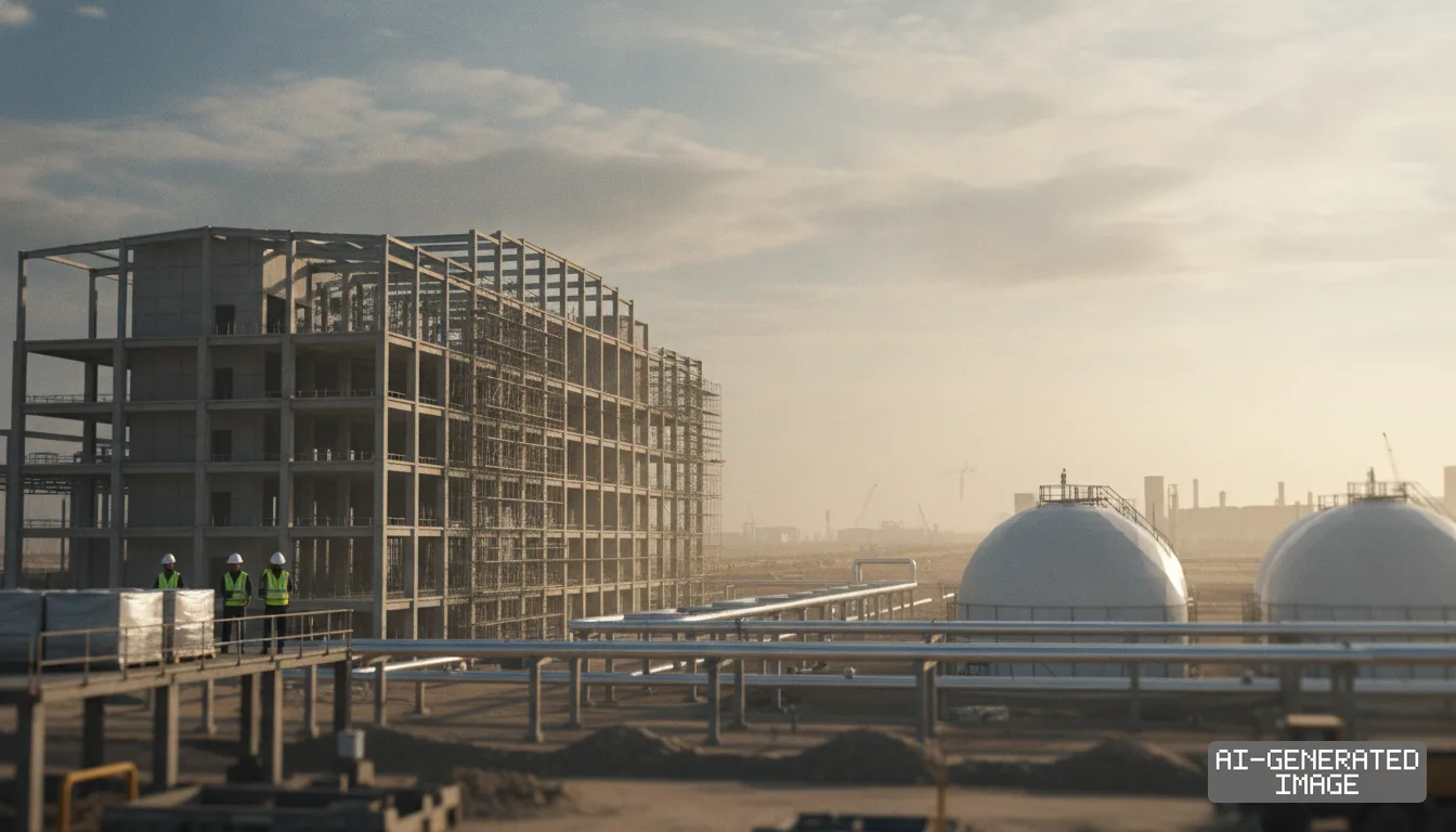
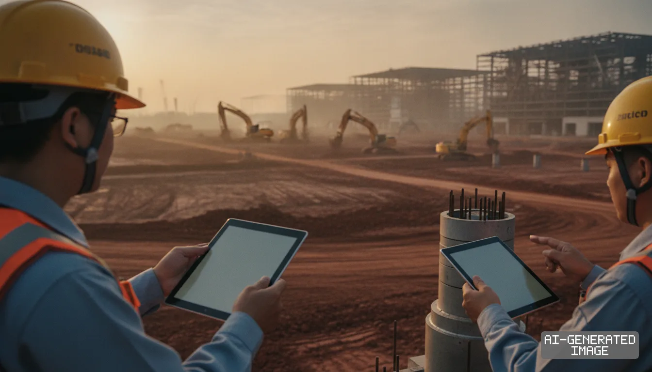
Under the newly cleared schedule, environmental impact assessments and statutory land reviews will run through 2028. Heavy civil engineering and groundbreaking on site are scheduled for 2030.
Taiwan Semiconductor Manufacturing Co. plans to commit more than NT$1 trillion ($31 billion) to the Longtan park. The investment covers three fabrication units dedicated to angstrom-era manufacturing.
Angstrom nodes represent the semiconductor generation below one nanometer, where transistor feature sizes require atomic-scale lithography. Volume production at the first Longtan facility is scheduled for 2030.
The Longtan campus provides physical room for architectures that follow TSMC's A14 process. The company formally unveiled the A14 node on April 23, 2025, targeting volume production in 2028.
TSMC revealed subsequent A13 and A12 designs on April 22, 2026. The company intends to shift those angstrom configurations into commercial operations during 2029, according to company roadmaps.
Initial A14 volume lines are already anchored at the Central Taiwan Science Park in Taichung. TSMC broke ground on that NT$1.5 trillion ($49 billion) Fab 25 project on Nov. 5, 2025.
Taichung absorbs the first wave of 1.4-nanometer capacity across four production modules. Longtan will take the subsequent node migrations as transistor structures move toward tighter physical limits, officials said.
Securing land two years before formal environmental approval locks in TSMC's long-term fab layout. Advanced logic fabrication plants require five to six years from site reservation to commercial production.
Foundry competition at the leading edge has narrowed to three global players. TSMC manufactures over 60% of all contract chips globally and more than 90% of advanced processors below five nanometers.
Intel Foundry is seeking external customers for its 18A and 14A nodes. Samsung Electronics is racing to deploy 2-nanometer gate-all-around transistor capacity to recapture leading-edge fab market share.
The Longtan approval gives TSMC designated domestic ground while overseas projects in Arizona and Kumamoto proceed. The company keeps its pioneer process development inside Taiwan before transferring formulas abroad.
Operating sub-1.4-nanometer facilities demands significant power and industrial water reserves. Science park authorities and the economics ministry are organizing dedicated high-voltage lines and water recycling plants for Taoyuan.
Water supply plans include local reclamation facilities to shield surrounding residential districts. The government committed to supplying treated wastewater directly to fab cooling towers, the development council said.
The Hsinchu Science Park Administration will supervise site acquisition after the national cabinet issues formal endorsement. Municipal officials in Taoyuan have pledged streamlined permits to maintain the 2030 target.
For fab equipment suppliers, the zoning decision confirms multi-year capital demand. Tool makers such as ASML, Applied Materials and Tokyo Electron face long delivery lead times for extreme ultraviolet equipment.
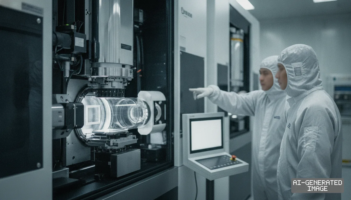
High-numerical-aperture extreme ultraviolet lithography systems are required for nodes below 1.4 nanometers. TSMC can now structure fab shell dimensions to house the larger scanner platforms at Longtan.
Customer commitments from Apple, Nvidia and AMD depend on predictable multi-year node cadence. By securing the site, TSMC signals to hyperscale buyers that fab floors will exist for future microarchitectures.
Next on the regulatory calendar, the draft plan goes to the Executive Yuan for final cabinet ratification. Detailed zoning amendments and municipal public hearings will open during the first half of 2027.
Environmental impact documentation must be submitted to the Ministry of Environment before the end of 2028. Public comment periods will follow statutory review sessions, according to the science council timeline.
The council notice does not state the precise construction timetable for individual fab shells. TSMC has not published a corporate filing specifying capex allocations for the Longtan parcel.
Impact map
How this development propagates across the region and out to global buyers.
| Event | Korea | China | Japan | Global impact |
|---|---|---|---|---|
| Longtan Phase 3 fab site approval | Samsung Electronics faces wider lead-time gap in sub-2nm foundry commercialization | Domestic foundries remain capped at mature nodes without extreme ultraviolet access | Equipment makers Tokyo Electron and Canon secure visibility on high-NA tool demand | Hyperscale chip buyers gain supply certainty for post-2029 angstrom-generation logic |
| Longtan Phase 3 fab site approval | Samsung Electronics faces wider lead-time gap in sub-2nm foundry commercialization | Domestic foundries remain capped at mature nodes without extreme ultraviolet access | Equipment makers Tokyo Electron and Canon secure visibility on high-NA tool demand | Hyperscale chip buyers gain supply certainty for post-2029 angstrom-generation logic |
In this story
- Companies
- TSMC
- Tickers
- 2330.TWTSM
- Exposed
- IntelSamsung ElectronicsASMLApplied MaterialsTokyo Electron
- Policy
- Economic SecuritySubsidies
- Impact
- CapexSupply ChainOrder Book
Track every Economic Security development → Track every Subsidies development →
Related briefings
- South Korea funds advanced chip packaging and backside power pilot lines Also on Applied Materials, Intel, Tokyo Electron
- Comparing East Asia Fab Subsidies Across Japan, Korea, and China Also on Applied Materials, ASML, Tokyo Electron
- SK hynix and foundries advance hybrid bonding for AI silicon in 2027 Also on Applied Materials, Intel, Tokyo Electron
- Tokyo Electron qualifies BSPDN coater-developer tracks for sub-2nm fabs Also on ASML, Intel, Tokyo Electron
Sources
Reporting
Confidence: medium — how we grade this
The documents behind this briefing are linked above. East Asia Brief produces its English text with AI assistance under human editorial review, and does not translate or republish other outlets' articles. See our methodology and AI policy. Spotted an error? Tell us.
The Morning Brief
What changed in Korean, Chinese and Japanese industry overnight — and what it means for your supply chain. One email, weekday mornings, US time. Free.
The first issue goes out shortly. Sign up now and you will not miss it.