Samsung opens Yokohama chip packaging lab to rival TSMC lead
The $280 million research site secures Japanese state subsidies to integrate domestic materials suppliers into Samsung's backend lines for AI accelerators and next-generation HBM.
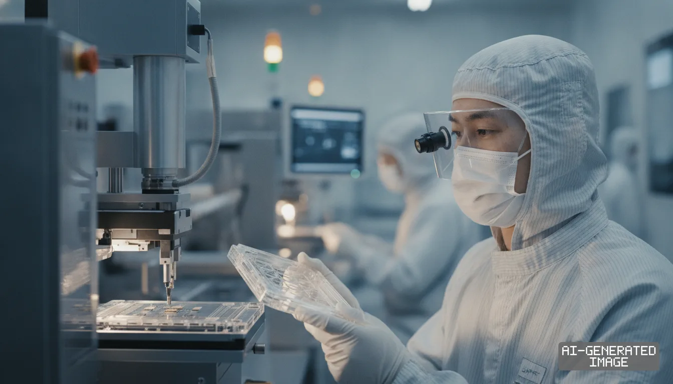
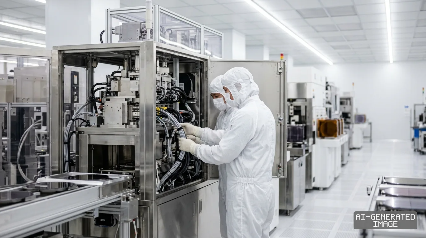
Samsung Electronics opened its Advanced Package Lab in Yokohama on Sept. 8, 2026, launching an advanced semiconductor packaging research facility to co-develop backend chip technologies with Japanese equipment and materials suppliers.
The South Korean chipmaker committed 40 billion yen ($280 million) over a five-year capital expenditure schedule running through 2028 to construct cleanrooms and install advanced packaging tools.
Japan's Ministry of Economy, Trade and Industry approved state subsidies of up to 22.5 billion yen ($157 million) for the project under its Post-5G information infrastructure enhancement initiative.
The municipal government of Yokohama contributed an additional 2.5 billion yen ($17 million) in local enterprise subsidies to support facility construction in its Minato Mirai 21 waterfront district.
Jun Young-hyun, vice chairman and head of the Device Solutions division at Samsung Electronics, attended the formal opening ceremony alongside roughly 100 Japanese government officials and industry executives.
Senior managers from 15 Japanese semiconductor supply-chain partners joined the opening ceremony, including representatives from chip equipment producer Tokyo Electron and integrated circuit substrate maker Ibiden.
Accelerating technical exchanges between South Korea and Japan will serve as the driving engine to jointly expand the next-generation packaging sector, Jun said during the opening ceremony.
The research center occupies roughly 6,600 square meters across repurposed floors of the Leaf Minato Mirai building, an office commercial property that Samsung Electronics purchased in Yokohama.
The facility houses cleanrooms engineered to mirror commercial production environments, allowing research engineers to test and qualify backend assembly machinery under volume manufacturing conditions.
About 95 research engineers from South Korea and Japan currently staff the Yokohama facility, focusing directly on advanced material validation and high-density heterogeneous chip assembly processes.
Samsung Electronics plans to expand that local engineering team to more than 100 specialists by late 2027, according to corporate investment filings submitted to Yokohama authorities.
Advanced packaging integrates discrete semiconductors — including graphics processing units and high-bandwidth memory (HBM) modules — onto a shared platform to multiply interconnect speed and cut latency.
Modern AI accelerators rely on 2.5D packaging architectures, where logic dies sit side by side on micro-etched silicon interposers to lower electrical resistance and heat buildup.
Taiwan Semiconductor Manufacturing Co. holds commanding control of this assembly market through its proprietary Chip-on-Wafer-on-Substrate technology, creating supply bottlenecks for global artificial intelligence processor designers.
Samsung Electronics operates as the only Asian chip manufacturer providing end-to-end turnkey services that combine advanced foundry wafer fabrication, memory production and backend packaging under single contracts.
Despite offering that consolidated production model, Samsung Electronics held a 5.9% share of the worldwide advanced packaging sector in 2024, trailing TSMC and dedicated packaging subcontractors.
The Yokohama facility seeks to close that competitive gap by placing Samsung engineers directly within Japan's dense manufacturing network of specialized chemical makers and precision equipment suppliers.
Japanese suppliers control more than 70% of the international market for specialized backend inputs, including protective epoxy resin molding compounds, dicing blades and biconcave substrate films.
The Yokohama laboratory will conduct joint engineering trials with Tokyo Electron on plasma dicing tools and precision wafer cleaning systems required for through-silicon via production.
Samsung Electronics also structured collaborative testing lines with Disco for precision wafer thinning, Namics for liquid underfill materials and Resonac for thermal interface adhesive films.
Direct testing in Yokohama reduces verification cycles for experimental materials from several months to several days, accelerating qualification schedules for upcoming sixth-generation HBM4 memory stacks.
HBM4 architectures alter packaging rules by replacing standard memory base dies with logic wafers produced on cutting-edge foundry nodes, requiring closer integration across supply lines.
The research center will also focus on high-density package substrates, an industry chokepoint where Japanese fabricator Ibiden maintains technical leadership in multi-layer coreless buildup panels.
Engineers in Yokohama are scheduled to develop System-on-Panel packaging, an alternate architecture that mounts silicon dies directly onto wide rectangular panels instead of circular wafer interposers.
Samsung Electronics also scheduled collaborative research with Japanese academic institutions, including the University of Tokyo, to develop novel heterogeneous interconnect architectures and train local packaging specialists.
By supporting Samsung's Advanced Package Lab, Japanese industrial planners ensure that domestic chemical formulators and machinery builders supply multiple competing international chipmakers rather than relying on a single foundry.
Samsung Electronics did not issue a public regulatory disclosure on the Korea Exchange or release a statement on its corporate newsroom regarding the Sept. 8 event.
Cleanroom testing and pilot tool calibrations will continue through the fourth quarter of 2026 as the five-year investment program proceeds toward its 2028 completion target.
Impact map
How this development propagates across the region and out to global buyers.
| Event | Korea | China | Japan | Global impact |
|---|---|---|---|---|
| Samsung Yokohama packaging lab launch | Samsung accelerates HBM4 validation; SK hynix faces tighter AI memory competition | Domestic foundries remain cut off from Japanese advanced packaging tooling under export controls | Tokyo Electron and Ibiden secure direct co-development on subsidized domestic pilot lines | AI accelerator designers gain secondary 2.5D packaging capacity beyond TSMC CoWoS bottlenecks |
In this story
- Companies
- Samsung Electronics
- Tickers
- 005930.KS
- Exposed
- TSMCTokyo ElectronIbidenResonacDisco
- Policy
- SubsidiesEconomic Security
- Impact
- Supply ChainCapexCost Structure
Track every Subsidies development → Track every Economic Security development →
Related briefings
- Japanese epoxy mold makers reformulate resins to tame warpage in 16-high memory Also on Resonac, Samsung Electronics, Cost Structure
- TSMC widens CoWoS supply chain with $2 billion US interposer deal Also on Disco, Tokyo Electron, Samsung Electronics
- Hanmi Semiconductor wins $18 million tool deal from Samsung Also on Disco
- Ibiden and Shinko ramp high-layer FC-BGA lines as AI server package sizes expand Also on Ibiden, Cost Structure, Subsidies
Sources
Reporting
Confidence: medium — how we grade this
The documents behind this briefing are linked above. East Asia Brief produces its English text with AI assistance under human editorial review, and does not translate or republish other outlets' articles. See our methodology and AI policy. Spotted an error? Tell us.
The Morning Brief
What changed in Korean, Chinese and Japanese industry overnight — and what it means for your supply chain. One email, weekday mornings, US time. Free.
The Morning Brief is in preparation. Leave your address and we will write to you once — when the first issue is ready. Nothing before that.