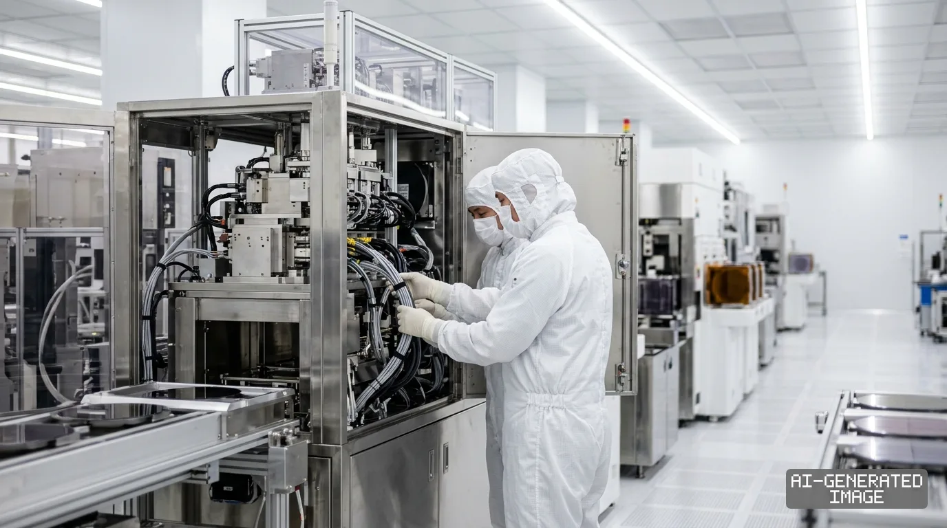
Samsung deploys TSMC-tested photonics probers for CPO push
The South Korean chipmaker deployed FormFactor and MPI probe stations to inspect optical wafers internally, aligning with TSMC standards to speed co-packaged optics commercialization.
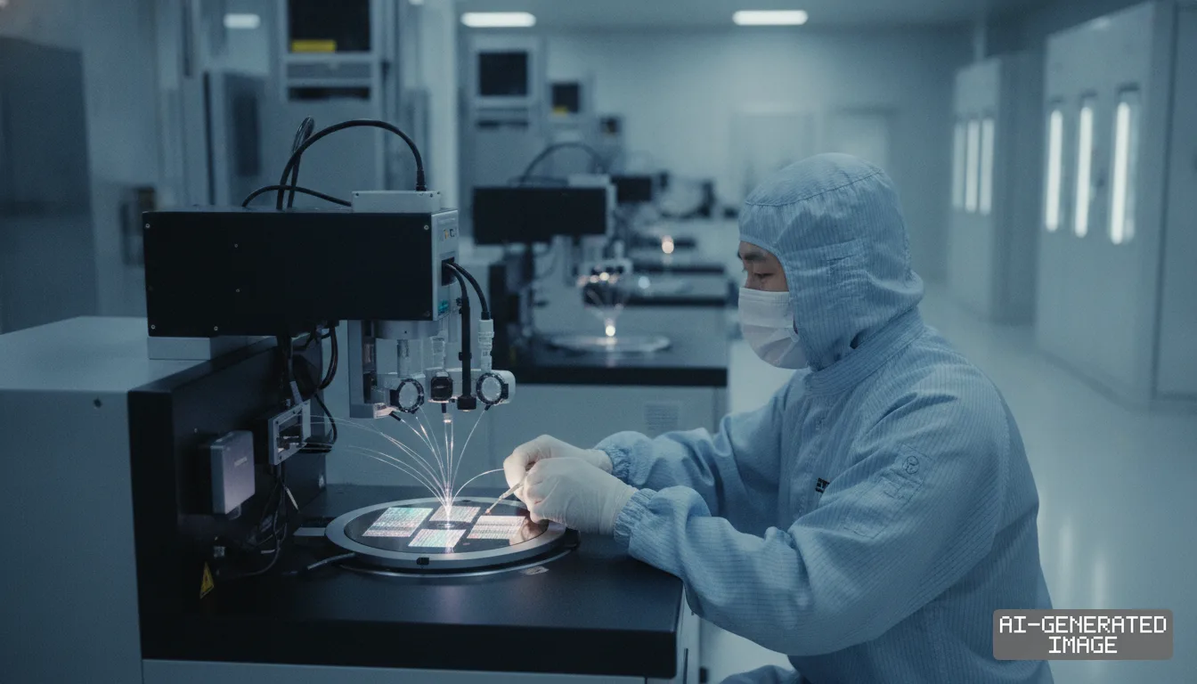
Samsung Electronics brought optical probe stations from FormFactor and MPI into its advanced packaging lines on Sept. 7, 2026, adopting wafer test tools qualified by rival TSMC.
The equipment allows Samsung to test photonic integrated circuits — semiconductor dies that transmit data using light instead of copper wires — at the wafer level before packaging.
Samsung previously outsourced PIC wafer evaluations to European research institute imec in Belgium. The purchase shifts that measurement work entirely inside its own semiconductor manufacturing lines.
FormFactor of the United States and MPI Corporation of Taiwan are the only two probe station suppliers qualified for TSMC’s Compact Universal Photonic Engine platform, known as COUPE.
TSMC developed COUPE to assemble co-packaged optics, or CPO. The packaging architecture mounts optical engines directly beside compute silicon on a shared substrate to cut latency and energy loss.
By installing the same probe stations, Samsung adopts the test baseline established by TSMC. The move prevents customer friction and cuts development cycles for its own optical foundry offerings.
Wafer-level optical testing is one of the steepest bottlenecks in manufacturing silicon photonics. Automated probe stations must align glass optical fibers to photonic ports on each die across an entire wafer.
A full optical and electrical inspection of a single photonic die takes more than 100 seconds. Conventional silicon logic chips require fractions of a second to test on production probe systems.
The testing bottleneck stems from mechanical alignment physics. An optical fiber has a core hundreds of times larger than an on-chip waveguide, requiring sub-micron motion control to prevent optical loss during measurement.
The probe stations connect to tunable lasers and electrical analyzers to sweep wavelengths. They measure whether fabricated optical modulators and photodiodes convert light and electricity without unexpected signal distortion.
Samsung aims to finish internal evaluations of PIC wafers using the FormFactor and MPI stations by the end of 2026, industry officials said.
The company had committed to launching its 300-millimeter silicon photonics foundry platform this year. Samsung unveiled that manufacturing schedule during the Optical Fiber Communication conference in Los Angeles in March.
Samsung confirmed it completed process design kits for optical customers, enabling fabless chip designers to submit tape-outs. The foundry platform uses 300-millimeter silicon-on-insulator wafers for photonic manufacturing.
Samsung plans to introduce standalone optical engines in 2027 and offer full turnkey CPO manufacturing by 2029. The roadmap targets optical interconnects inside hyperscale artificial intelligence clusters.
Samsung Foundry secured its first commercial order from a major optical transceiver supplier earlier this year. Production under that supply agreement begins in the second half of 2026, the company said.
The transition to optical interconnects addresses power limits in artificial intelligence hardware. Traditional copper wiring cannot transfer massive data volumes between processors and memory without generating unmanageable heat.
Co-packaged optics replaces traditional pluggable optical transceivers positioned on server chassis faceplates. Placing optical engines millimeters away from switch and accelerator silicon cuts electrical trace resistance and power draw.
Co-packaged optics production involves multiple testing insertions. Foundries must test bare PIC wafers, test electronic control dies, verify bonded optical engines and validate final assembled modules under thermal burn-in.
By bringing PIC wafer testing in-house, Samsung secures the initial insertion point of the flow. Screening defective optical dies before packaging prevents wasting expensive logic chips and high-bandwidth memory.
Samsung operates memory fabs, logic foundries and packaging plants under a single company. TSMC relies on external memory partners like SK hynix to deliver high-bandwidth memory for packaged AI accelerators.
Samsung is pitching that full-stack model to win optical packaging customers from TSMC. It aims to integrate custom logic, high-bandwidth memory and optical engines on unified substrates without coordinating separate vendors.
TSMC plans to begin volume manufacturing of CPO components using its COUPE platform by late 2026. The Taiwanese foundry has aligned with major semiconductor designers including Nvidia to standardize optical engines.
Developing proprietary optical testing standards would have delayed Samsung's commercial schedule. Adopting FormFactor and MPI tools allows Samsung to match the testing environment that major chip designers already trust.
Neither Samsung, FormFactor nor MPI disclosed order values or the volume of probe stations installed. Samsung also declined to identify the specific advanced packaging fab operating the new tools.
Impact map
How this development propagates across the region and out to global buyers.
| Event | Korea | China | Japan | Global impact |
|---|---|---|---|---|
| optical probe adoption | in-house PIC testing | — | — | standardized CPO test |
In this story
- Companies
- Samsung ElectronicsTaiwan Semiconductor Manufacturing Co.FormFactorMPI Corporation
- Tickers
- 005930.KS2330.TWFORM3504.TW
- Exposed
- Nvidia
- Policy
- SubsidiesEconomic Security
- Impact
- Supply ChainCapexCompliance
Track every Subsidies development → Track every Economic Security development →
Related briefings
- TSMC weighs Texas fab campus to broaden US foundry footprint Also on Taiwan Semiconductor Manufacturing Co., Nvidia, Samsung Electronics
- TSMC widens CoWoS supply chain with $2 billion US interposer deal Also on Taiwan Semiconductor Manufacturing Co., Nvidia, Samsung Electronics
- GlobalFoundries agrees to build silicon interposers for TSMC in $2B deal Also on Taiwan Semiconductor Manufacturing Co., Nvidia, Samsung Electronics
- TSMC warns AI cannot solve physical barriers for 1.4nm chips Also on Taiwan Semiconductor Manufacturing Co, Nvidia, Samsung Electronics
Sources
Reporting
Confidence: medium — how we grade this
The documents behind this briefing are linked above. East Asia Brief produces its English text with AI assistance under human editorial review, and does not translate or republish other outlets' articles. See our methodology and AI policy. Spotted an error? Tell us.
The Morning Brief
What changed in Korean, Chinese and Japanese industry overnight — and what it means for your supply chain. One email, weekday mornings, US time. Free.
The Morning Brief is in preparation. Leave your address and we will write to you once — when the first issue is ready. Nothing before that.