Taiwan breaks ground on TSMC packaging base to relieve CoWoS limits
The 88.7-hectare Baipu park will host tool-validation labs and supplier lines to ease advanced chip packaging constraints for AI processors.
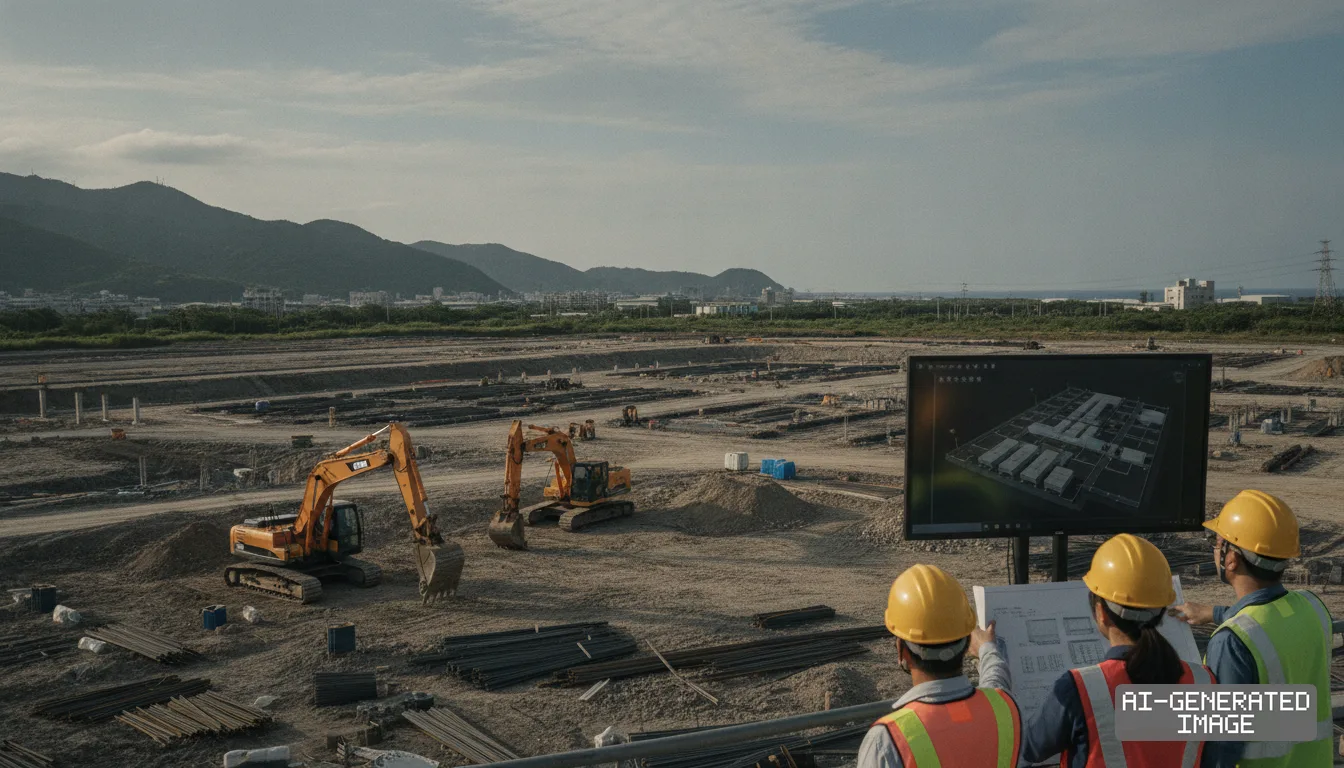
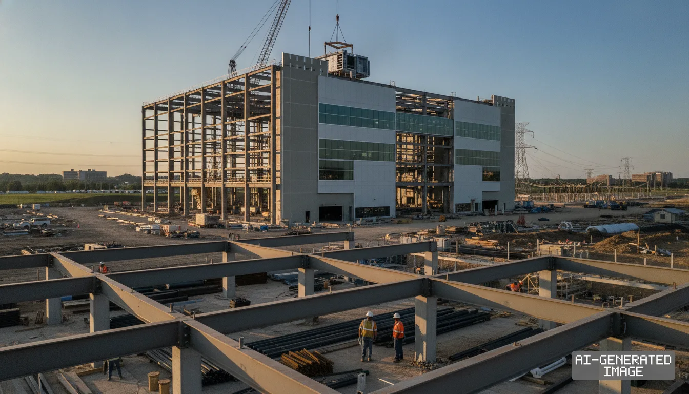
Taiwanese authorities broke ground Sept. 21, 2026 on the Baipu Industrial Park in Kaohsiung, establishing an advanced packaging base to ease capacity bottlenecks for artificial intelligence processors.
The 88.73-hectare development allocates 53.63 hectares for industrial use, the Kaohsiung City Government said. Around 25 hectares, or roughly 47% of that industrial space, is reserved for back-end semiconductor equipment and materials vendors.
Officials project the site will generate 300 billion New Taiwan dollars ($9.4 billion) in annual output value. The park is planned to create over 4,000 local technical jobs.
The hub addresses severe shortages in Chip-on-Wafer-on-Substrate packaging, known as CoWoS. Advanced packaging combines logic dies and high-bandwidth memory side by side, forming the central manufacturing hurdle for AI hardware.
Taiwan Semiconductor Manufacturing Co. will anchor the dedicated zone. TSMC plans to develop a 3-hectare plot housing two facilities: a technology validation laboratory and a specialized talent-training center.
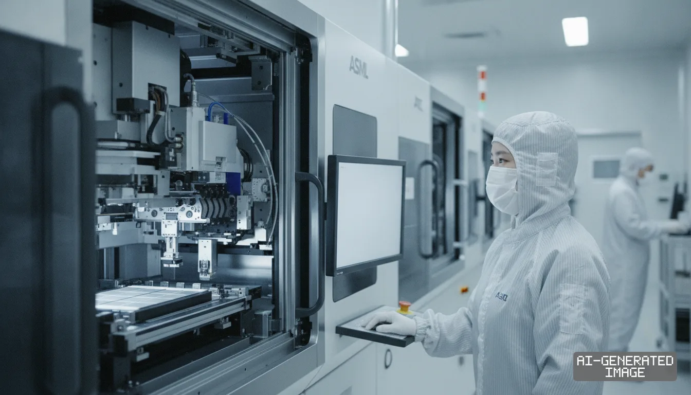
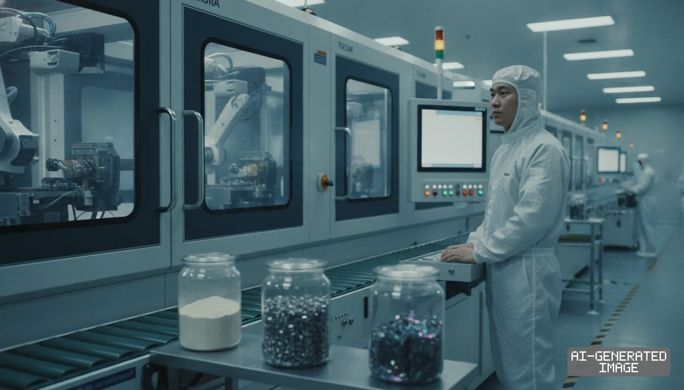
The validation facility will feature modular lines with clean rooms and test bays, TSMC Vice President Jun He said. The infrastructure allows suppliers to test machinery and materials before shipping tools to high-volume manufacturing fabs.
The on-site platform will shorten engineering iterations and improve packaging validation efficiency by 25% to 50%, He said. TSMC projects its total CoWoS production capacity will grow at an annual compound rate exceeding 80% through 2027.
Customer commitments from Nvidia and Advanced Micro Devices have driven the expansion. Both chip designers rely almost entirely on TSMC for turnkey foundry processing and high-density 2.5D packaging integration.
Taiwan President Lai Ching-te attended the opening event alongside TSMC Co-Chief Operating Officer Y.P. Chin and ASE Technology Holding Chief Executive Tien Wu. The presence of rival outsourcing firms underscores an island-wide effort to align the supply chain.
ASE operates packaging and testing facilities in nearby Renwu. Integrating ASE and TSMC back-end networks aims to prevent tool redundancy and secure intermediate substrate availability across southern Taiwan.
Baipu serves as a junction within Taiwan's southern semiconductor corridor. The zone connects TSMC's 2-nanometer wafer fab in Nanzih with precision materials suppliers located in Qiaotou.
Taiwan's Ministry of Economic Affairs formally approved the industrial zone on March 17, 2026. Local planners selected civil engineering contractors earlier in the month before authorizing earthworks.
More than 20 semiconductor supply-chain vendors attended the ceremony to review industrial plot allocations, according to municipal filings. The municipal administration has already initiated planning for an adjacent phase-two expansion.
The Ministry of Economic Affairs did not disclose the direct capital expenditure figure for TSMC's validation facilities. TSMC has not published a standalone corporate filing regarding the project on its investor relations platform.
Construction of municipal utilities and core road networks will continue through early 2028. TSMC's validation laboratories and training facilities are scheduled to begin formal operations in the fourth quarter of 2029.
Impact map
How this development propagates across the region and out to global buyers.
| Event | Korea | China | Japan | Global impact |
|---|---|---|---|---|
| Baipu advanced packaging hub | Samsung and SK hynix face wider packaging lead times as TSMC binds tool ecosystem | Domestic foundries lack access to high-efficiency 2.5D modular validation lines | Tokyo Electron and packaging chemical makers secure direct qualification sites | AI accelerator delivery schedules ease as packaging qualification cycle tightens |
In this story
- Companies
- Taiwan Semiconductor Manufacturing CoASE Technology Holding
- Tickers
- 2330.TW3711.TW
- Exposed
- NvidiaAdvanced Micro Devices
- Policy
- SubsidiesEconomic Security
- Impact
- Supply ChainCapexOrder Book
Track every Subsidies development → Track every Economic Security development →
Related briefings
- Silicon interposer scaling drives foundry and OSAT shifts in 3.5D chiplets Also on ASE Technology Holding, Advanced Micro Devices, Taiwan Semiconductor Manufacturing Co
- JCET expands automotive radar SiP packaging lines to capture ADAS sensor demand Also on ASE Technology Holding, Order Book
- AMD Reaffirms TSMC Alliance While Evaluating Rival Foundries Also on Advanced Micro Devices, Taiwan Semiconductor Manufacturing Co.
- Ibiden and Shinko ramp high-layer FC-BGA lines as AI server package sizes expand Also on Advanced Micro Devices, Order Book
Sources
Reporting
Confidence: medium — how we grade this
The documents behind this briefing are linked above. East Asia Brief produces its English text with AI assistance under human editorial review, and does not translate or republish other outlets' articles. See our methodology and AI policy. Spotted an error? Tell us.
The Morning Brief
What changed in Korean, Chinese and Japanese industry overnight — and what it means for your supply chain. One email, weekday mornings, US time. Free.
The Morning Brief is in preparation. Leave your address and we will write to you once — when the first issue is ready. Nothing before that.