Samsung Electro-Mechanics commits $3.1B to Sejong AI chip plant
The 4.27-trillion-won package substrate expansion targets completion by May 2028 to supply flip-chip components for artificial intelligence servers.
Samsung Electro-Mechanics affirmed plans Nov. 16, 2026, to spend 4.27 trillion won ($3.1 billion) expanding high-density flip-chip package substrate capacity at its Sejong complex for artificial intelligence servers.
The capital expenditure represents 43.6% of the company's 9.797 trillion won equity base. It marks the largest single-product factory investment in the firm's history, according to regulatory filings.
South Korea's Ministry of Trade, Industry and Energy published the facility roadmap Nov. 16 following a regional mega-project review in Asan. The Sejong expansion forms the first stage of an eight-trillion-won regional manufacturing blueprint.
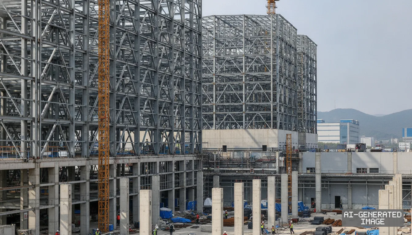
The factory will occupy the Myeonghak Industrial Complex in Sejong. Plans call for a four-story structure enclosing roughly 99,000 square meters of production floor, the company said.
The board approved the domestic project on Sept. 28, alongside a companion investment in Southeast Asia. Directors authorized 2.51 trillion won for the company's Vietnamese production subsidiary, bringing aggregate substrate outlays to 6.78 trillion won.
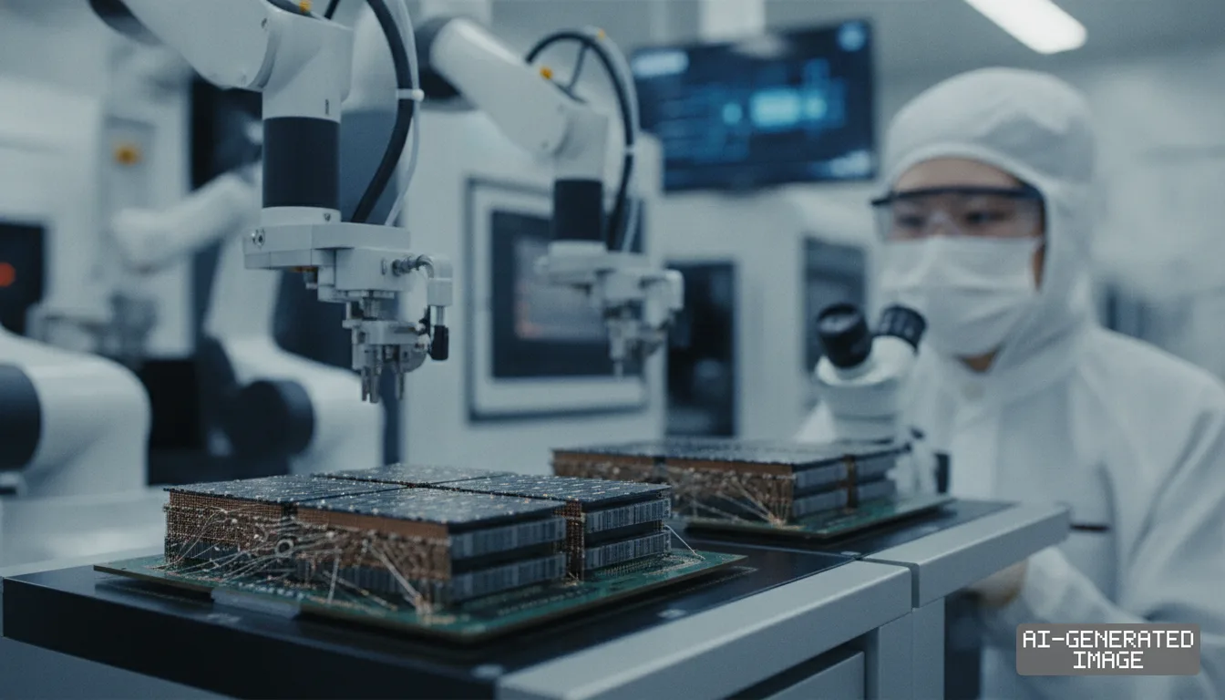
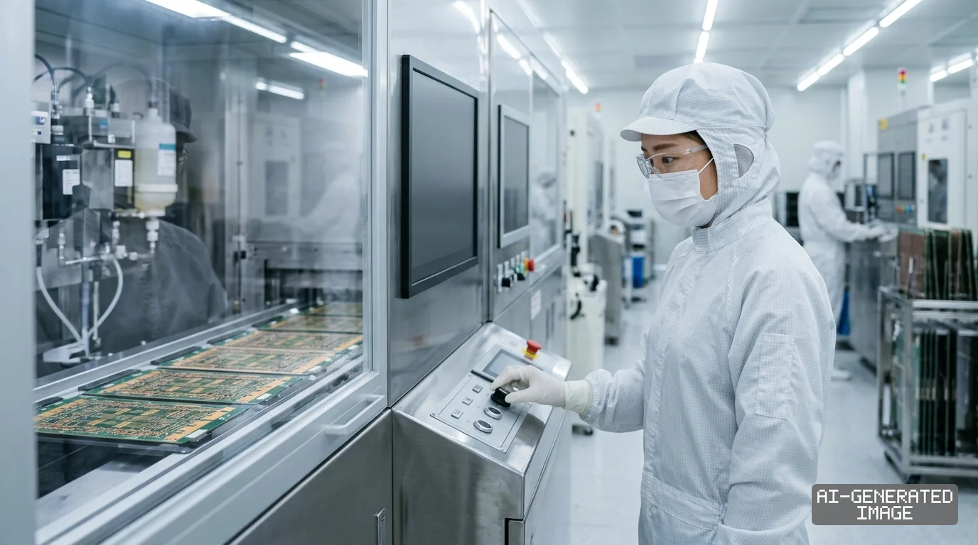
The Sejong lines will produce flip-chip ball grid array (FC-BGA) substrates. The multi-layer components route microscopic electrical signals and power between computing silicon dies and system motherboards.
High-performance artificial intelligence processors require substrates with more than 20 built-up circuit layers. By contrast, conventional personal computer processors typically rely on substrates containing between six and 10 layers.
Substrate surface areas have also expanded beyond 70 by 70 millimeters to accommodate massive accelerator packages. The packages combine central processing units, graphics engines and multiple high-bandwidth memory stacks on a single module.
Those expanding package footprints have created a severe manufacturing bottleneck across the semiconductor industry. Larger substrate dimensions raise the risk of warping during thermal baking steps, reducing fabrication yields at packaging lines.
Samsung Electro-Mechanics signed a supply agreement with Nvidia on Oct. 21 to address the packaging shortfall. The deal reserves dedicated manufacturing capacity in Sejong and Busan, with initial substrate shipments scheduled for late 2026.
The supplier is positioning itself to satisfy growing custom silicon demand among North American cloud computing platforms. Leading hyperscale data center operators have begun designing proprietary artificial intelligence accelerators to limit dependence on standard graphics processors.
Cloud hyperscalers require larger substrate panels that integrate specialized chiplets through advanced packaging. Fabricating those panels requires precise laser-drilling equipment capable of etching microscopic via holes across dozens of dielectric resin sheets.
The Sejong expansion challenges Japanese market leaders Ibiden and Shinko Electric Industries. The two Japanese manufacturers currently control roughly 60% of the global market for high-end server-grade FC-BGA substrates.
Japanese competitors have largely committed their high-layer production output to long-term enterprise customers through 2027. That tight capacity allocation has forced secondary chip designers to seek alternative qualified substrate vendors across East Asia.
Production relies heavily on Ajinomoto Build-up Film, an insulating epoxy resin film supplied by Japan's Ajinomoto. The proprietary film insulates the dense micro-circuits stacked between the multiple conduction layers of each FC-BGA package.
Surging server accelerator sizes have multiplied film consumption per package across the industry. Substrate makers must balance raw dielectric material deliveries against machine installation timelines to maintain continuous line operations.
Samsung Electro-Mechanics structured the capital outlay around binding multi-year customer purchase orders. Upfront financial contributions from primary corporate buyers will help offset equipment depreciation expenses as photolithography tooling arrives, the company said.
The investment also strengthens domestic semiconductor packaging capability under South Korea's broader advanced packaging initiative. Component makers and contract packaging houses are forming tighter regional manufacturing links to support domestic foundries and memory suppliers.
The Sejong municipal government modified local industrial park zoning rules to clear site access. Municipal planners realigned public utility rights-of-way and expedited environmental reviews to compress the initial engineering schedule.
Regional authorities also coordinated high-voltage electricity feeds and industrial water links to support round-the-clock cleanroom operations. Local utility contracts were adjusted to accommodate the heavy power draw required by advanced laser-drilling tools.
Capital deployment for the Sejong facility runs through May 31, 2028, according to company disclosure filings. Samsung Electro-Mechanics scheduled commercial mass production at the site to begin in September 2028.
The companion facility in Thai Nguyen, Vietnam, operates under a longer project timeline. Samsung Electro-Mechanics aims to complete installation and begin volume substrate processing at the overseas subsidiary by June 2030.
Company regulatory filings and ministry briefings do not confirm reported customer-specific cost-sharing terms or dedicated production lines for electric vehicle manufacturer Tesla, leaving bilateral automotive packaging supply arrangements formally undisclosed.
Impact map
How this development propagates across the region and out to global buyers.
| Event | Korea | China | Japan | Global impact |
|---|---|---|---|---|
| Sejong FC-BGA expansion | Samsung Electro-Mechanics commits 4.27 trillion won, 43.6% of equity | Cloud server builders face tighter packaging allocation until 2028 | Ibiden and Shinko Electric defend ~60% market share as Ajinomoto supplies ABF | AI accelerator module packaging bottlenecks ease with volume output in September 2028 |
In this story
- Companies
- Samsung Electro-Mechanics
- Tickers
- 009150.KS
- Exposed
- NvidiaIbidenShinko Electric IndustriesAjinomoto
- Impact
- CapexSupply ChainOrder Book
Related briefings
- Ibiden and Shinko ramp high-layer FC-BGA lines as AI server package sizes expand Also on Ajinomoto, Shinko Electric Industries, Ibiden
- South Korean substrate makers develop embedded silicon bridges for AI chips Also on Shinko Electric Industries, Ibiden, Samsung Electro-Mechanics
- Nvidia and Tesla fund $2.8B Samsung Electro-Mechanics lines Also on Ibiden, Samsung Electro-Mechanics, Nvidia
- Doosan commits $397 million to China advanced chip packaging materials Also on Ibiden, Samsung Electro-Mechanics, Nvidia
Sources
Primary documents
Reporting
Confidence: high — how we grade this
The documents behind this briefing are linked above. East Asia Brief produces its English text with AI assistance under human editorial review, and does not translate or republish other outlets' articles. See our methodology and AI policy. Spotted an error? Tell us.
The Morning Brief
What changed in Korean, Chinese and Japanese industry overnight — and what it means for your supply chain. One email, weekday mornings, US time. Free.
The Morning Brief is in preparation. Leave your address and we will write to you once — when the first issue is ready. Nothing before that.