SK hynix speeds HBM4 design with Nvidia physics simulation tools
The system cuts chip thermal and deformation runtime by over 30 times compared to a 32-thread CPU, shortening custom AI server memory cycles.
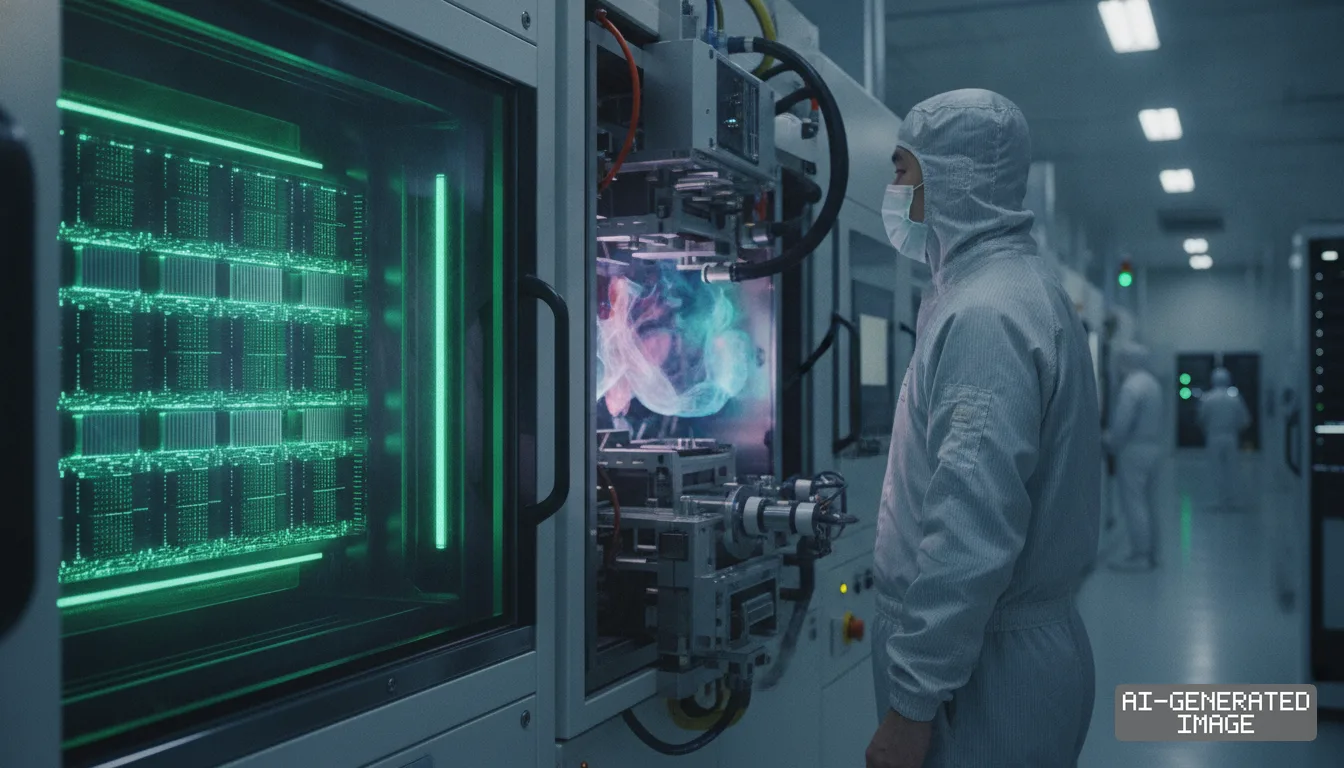
SK hynix expanded its deployment of Nvidia-accelerated simulation platforms on Nov. 11, 2026, using graphics hardware to shorten development cycles for custom High Bandwidth Memory 4 stacks bound for AI servers.
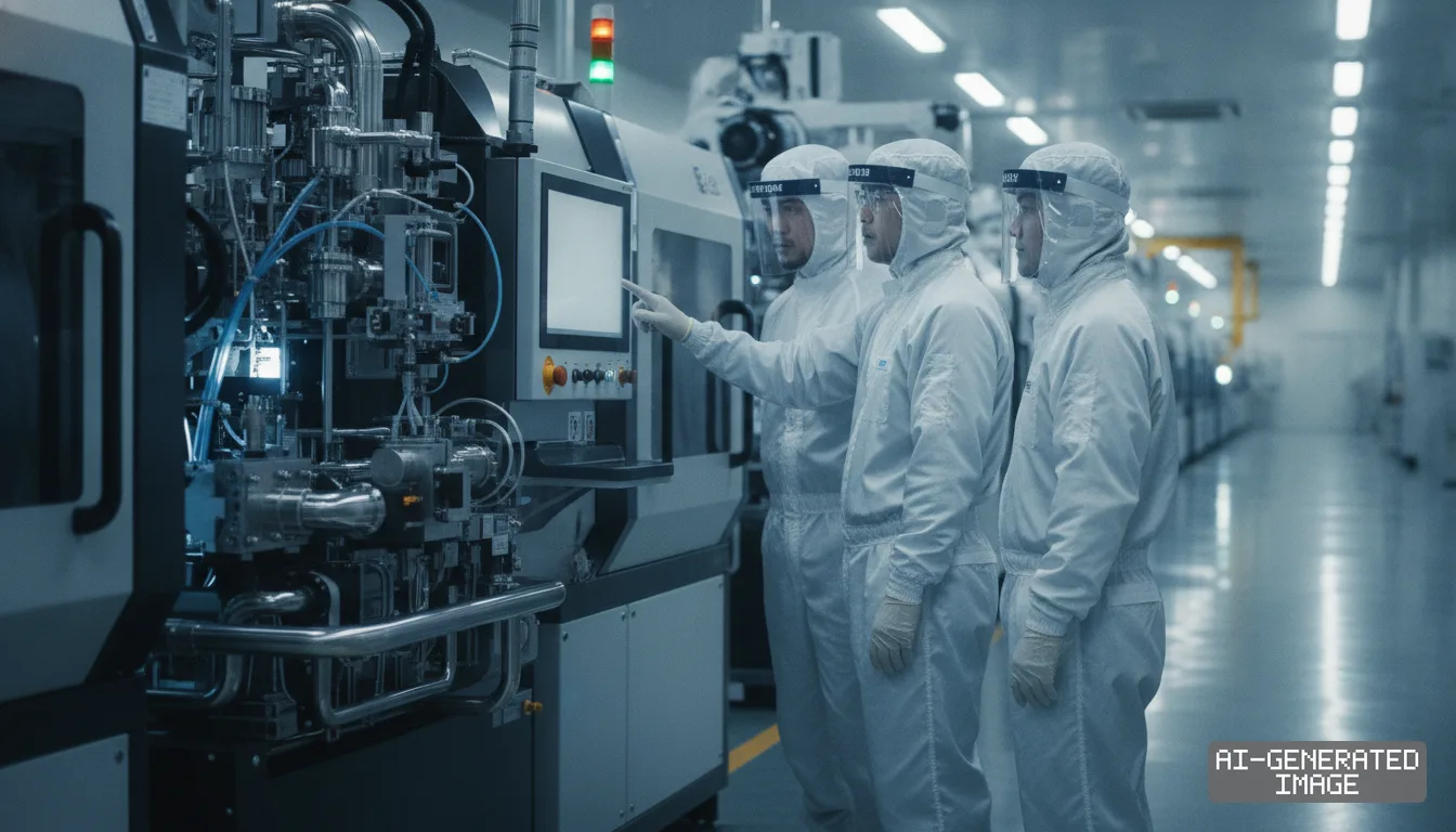
The new system cuts chip-scale thermal and mechanical deformation simulation times by more than 30 times compared to a 32-thread central processing unit. Gas etch modeling accelerated dozens of times over traditional runtimes, the company said.
The memory maker uses Nvidia CUDA-X libraries, CuPy and cuBLAS alongside the PhysicsNeMo physics-simulation framework. Those tools form the core of TCAD 3.0, an internal platform developed at the SK hynix Future Technology Research Institute.
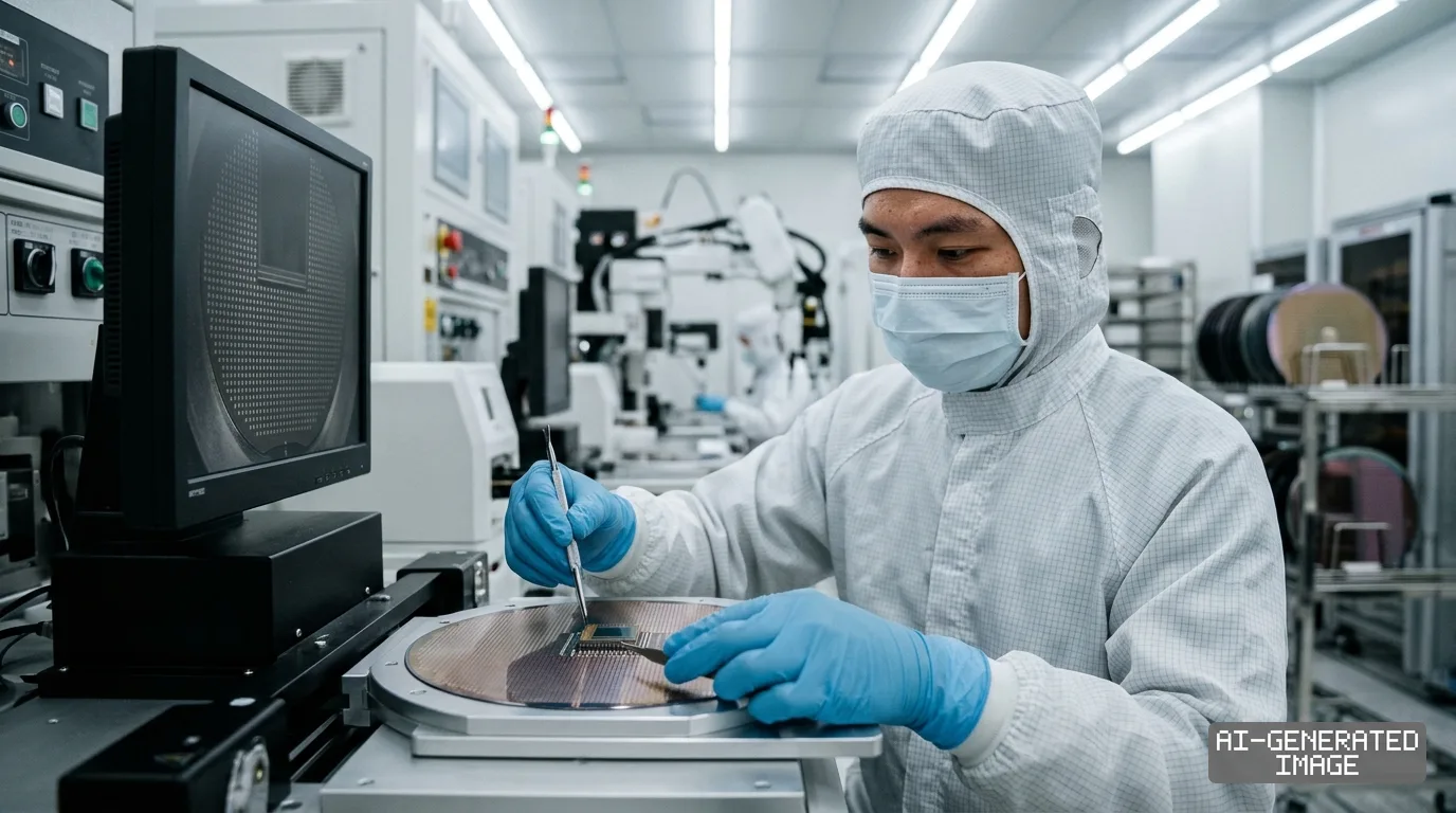
Technology Computer-Aided Design, or TCAD, models how physical structures take shape during wafer fabrication. Virtual manufacturing allows semiconductor engineers to test transistor behavior and chemical processes in software before committing wafers to fabrication lines.
Advanced memory requires far more simulation than earlier planar DRAM. High Bandwidth Memory stacks multiple dynamic random-access memory dies vertically, connecting them through thousands of microscopic copper pillars called through-silicon vias.
Stacking dies traps heat and creates mechanical warping as chips expand at different rates during operation. Solving those physical equations across an entire multi-die package previously required weeks of server compute time, delaying design sign-off.
Gas etching poses a second computational barrier. The chemical process carves deep trenches into silicon across five or more distinct steps, creating billions of geometric permutations that conventional simulators struggle to calculate without physical test runs.
SK hynix trained surrogate neural-network models using PhysicsNeMo to predict profile changes during etching. The surrogate models generate synthetic training data that fill gaps where empirical test wafers are missing, reducing physical trial runs.
The engineering team applies cuBLAS and CuPy to solve dense linear systems in parallel. Moving the thermal matrix equations from central processors onto graphics accelerators eliminated numerical bottlenecks that previously restricted simulation to partial chip cross-sections.
Full-chip structural modeling now completes in hours rather than days. That allows packaging teams to evaluate dozens of bump pitches and underfill adhesives before freezing die layouts, cutting physical re-masking costs.
The simulation work builds on a multiyear technology partnership that SK hynix and Nvidia announced on June 8, 2026. That agreement committed both companies to co-developing custom memory architectures and factory digital twins.
Nvidia relies heavily on the South Korean chipmaker to furnish high-speed memory for its computing platforms. Industry analysts estimate SK hynix supplies roughly 70% of the advanced HBM modules used in Nvidia AI accelerators.
Memory specifications are shifting as customers demand bespoke silicon. While earlier generations used standard commodity base dies, HBM4 adopts logic base dies fabricated on advanced foundry processes, requiring co-design between memory makers, foundries and system architects.
SK hynix has partnered with Taiwan Semiconductor Manufacturing Co. to manufacture the base dies for its HBM4 products. The tighter physical tolerances of sub-four-nanometer logic dies make package-level thermal simulation mandatory before taping out.
Conventional simulation tools must adapt as memory becomes customized, Kim Jung-han, head of the TCAD intelligence team at SK hynix, said during an engineering presentation in Seoul. Combining AI physics with numerical solvers overcomes computational boundaries, he said.
The engineering team is also connecting physics simulation to factory digital twins built on Nvidia Omniverse software. That integration models cleanroom airflow, automated material handling and chemical distribution before installation inside new Korean fabrication lines.
Domestic rival Samsung Electronics is running similar GPU-accelerated simulation programs. Samsung works with Nvidia cuISS and cuDSS solvers for sparse matrices, cutting chip-scale thermal analysis time from 18 hours to 41 seconds on test workloads.
The shift toward accelerated electronic design automation reflects a broader industry bottleneck. As physical scaling slows, chipmakers must extract performance gains through complex 3D integration, increasing computing demands on design departments.
SK Group is aligning its broader infrastructure investments with the hardware architecture. The group signed an agreement on July 25, 2026, to deploy Nvidia Vera Rubin systems within a planned 2-gigawatt cloud facility operated by SK Telecom.
SK hynix did not disclose the capital expenditure committed to the GPU clusters running TCAD 3.0. Furthermore, neither company filed an exchange disclosure on Nov. 11 establishing revised pricing or minimum volume commitments.
Commercial HBM4 shipments for Nvidia Vera Rubin AI platforms begin in the second half of 2026, ahead of broader datacenter cluster deployments scheduled across 2027.
Impact map
How this development propagates across the region and out to global buyers.
| Event | Korea | China | Japan | Global impact |
|---|---|---|---|---|
| GPU-accelerated TCAD adoption | SK hynix shortens custom HBM4 design loops, securing ~70% Rubin share | CXMT remains reliant on legacy 2D EDA tools, widening HBM gap to 3 years | Tokyo Electron integrates GPU-based simulation models into dry etch tool recipes | AI server tape-out lead times fall 15-20% on faster thermal sign-off |
In this story
- Companies
- SK hynixNvidia
- Tickers
- 000660.KSNVDA
- Exposed
- Samsung ElectronicsTaiwan Semiconductor Manufacturing Co.
- Impact
- Supply ChainCapexCost Structure
Related briefings
- Intel pits EMIB-T packaging against TSMC to win AI chip orders Also on Taiwan Semiconductor Manufacturing Co., Nvidia, SK hynix
- GlobalFoundries signs $2 billion TSMC chip interposer deal Also on Taiwan Semiconductor Manufacturing Co., Nvidia, SK hynix
- TSMC and Samsung unify 3nm base die specs for Nvidia custom HBM Also on Taiwan Semiconductor Manufacturing Co., Nvidia, SK hynix
- TSMC reviews vertical 3D DRAM production after Nvidia request Also on Taiwan Semiconductor Manufacturing Co., Nvidia, SK hynix
Sources
Primary documents
Reporting
Confidence: high — how we grade this
The documents behind this briefing are linked above. East Asia Brief produces its English text with AI assistance under human editorial review, and does not translate or republish other outlets' articles. See our methodology and AI policy. Spotted an error? Tell us.
The Morning Brief
What changed in Korean, Chinese and Japanese industry overnight — and what it means for your supply chain. One email, weekday mornings, US time. Free.
The Morning Brief is in preparation. Leave your address and we will write to you once — when the first issue is ready. Nothing before that.