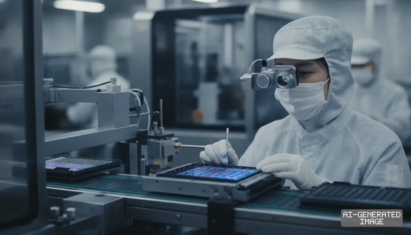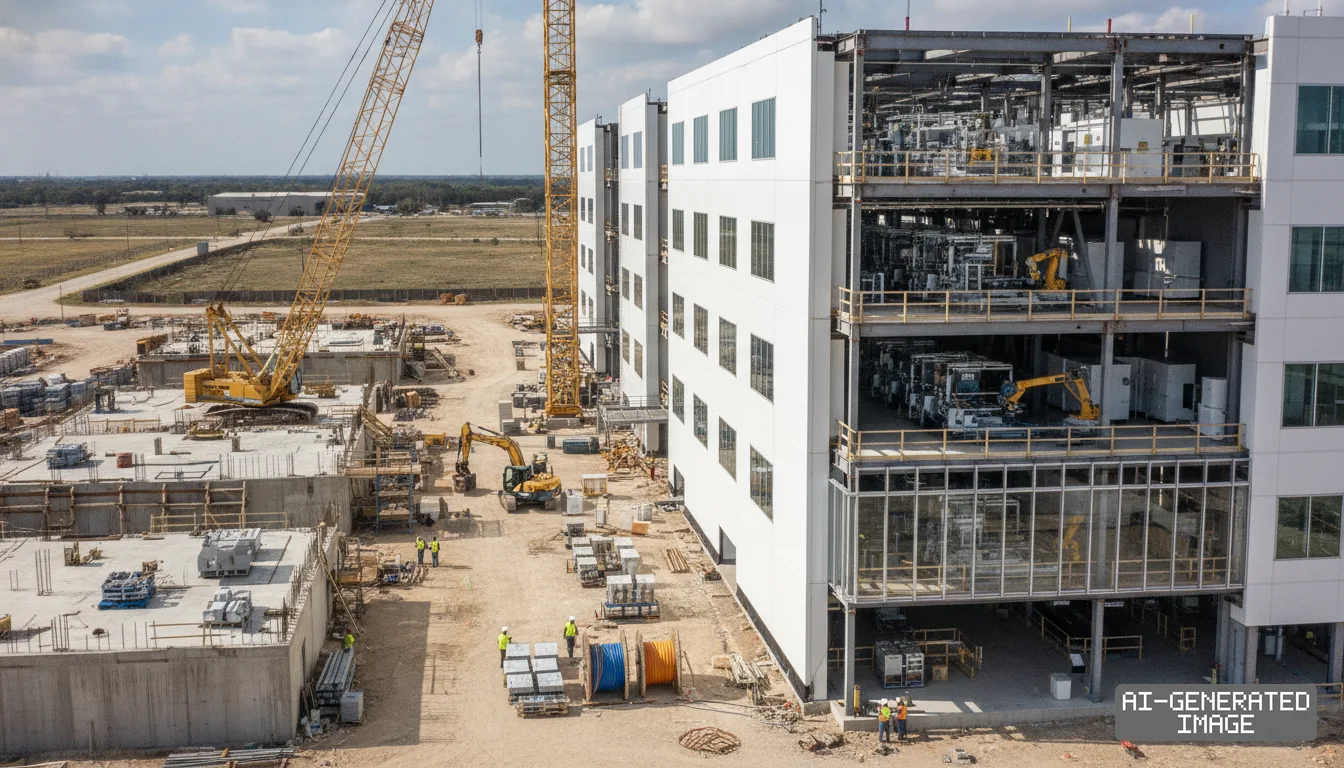
Intel pits EMIB-T packaging against TSMC to win AI chip orders
The US chipmaker claims 90% wafer utilization for its embedded silicon bridge, targeting a projected 20% packaging deficit at TSMC.
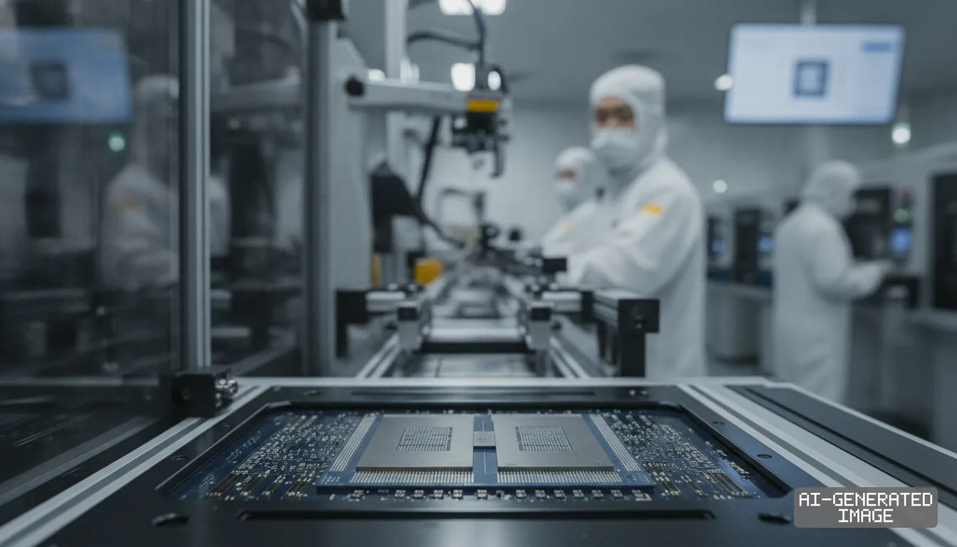
Intel presented its EMIB-T packaging roadmap on Nov. 5, 2026, pitching its bridge architecture against TSMC's CoWoS-L to secure fabless customers facing severe advanced packaging bottlenecks.
The technology addresses the primary capacity pinch point in artificial intelligence infrastructure. Taiwan Semiconductor Manufacturing Co. (TSMC) controls roughly 95% of leading-edge 2.5D packaging capacity, creating a projected 15% to 20% supply shortfall through 2027.
Intel claims silicon wafer utilization exceeds 90% when embedding miniature silicon bridges directly into substrates. In contrast, full silicon interposers achieve roughly 60% wafer utilization, according to data presented by Intel packaging executives.
Lee Kyu-oh, packaging director at Intel Foundry, outlined the economic comparison on Nov. 5 at the International Symposium on Microelectronics Packaging in Busan. Placing silicon only where connections are needed sharply lowers material overhead, Lee said.
TSMC builds its competing CoWoS-L architecture by inserting passive silicon bridges inside an organic interposer. Intel embeds its bridges directly into the organic package substrate, eliminating the interposer layer entirely to reduce substrate warpage.
EMIB-T adds through-silicon vias — vertical electrical connections etched directly through silicon — into each bridge. The vertical vias provide direct power delivery and signal paths, resolving voltage drop issues that limited earlier bridge generations.
The upgraded bridges incorporate metal-insulator-metal capacitors to suppress power noise during sudden computing load spikes. The design allows high-bandwidth memory stacks to receive clean voltage without bulky external decoupling capacitors, the company said.
Intel engineers demonstrated a first-level interconnect bump pitch scaling down to 25 µm in technical papers. That interconnect density supports data transmission rates reaching 64 gigabits per second across Universal Chiplet Interconnect Express interfaces.
The bridge architecture is engineered to support next-generation memory standards, including HBM4 and HBM4e. The interfaces achieve data transfer rates exceeding 12 gigabits per second, matching the thermal and signal specifications of high-performance accelerators.
Package dimensions can expand up to 120 by 120 mm under the architecture, Intel technical papers show. That footprint accommodates more than nine reticle sizes of compute and memory silicon, connected by over 20 embedded bridges.
Roadmap projections target package sizes reaching 120 by 180 mm and eventually 240 by 240 mm, Lee said. The largest multi-die systems will require more than 32 memory stacks interconnected by over 70 individual silicon bridges.
Thermal performance benefits from the smaller silicon footprint, the company said. Reduced thermal expansion mismatch between the silicon bridges and the organic substrate allows the package to support thermal design power levels exceeding 1,000 watts.
Leading AI accelerator designers face acute packaging allocation constraints across East Asia. Nvidia consumes roughly half of TSMC's available CoWoS packaging volume, leaving competing designers and cloud hyperscalers with production lead times stretching beyond 50 weeks.
Google and Amazon are evaluating EMIB-T for proprietary data center accelerators, supply chain analysts said. Both cloud service providers seek alternative manufacturing routes to prevent packaging quotas from capping their internal server deployments.
Memory makers SK hynix and Samsung Electronics are testing interface compatibility between their HBM4 base dies and Intel's packaging lines. Direct qualification would allow memory vendors to supply processors packaged outside TSMC's ecosystem.
Substrate procurement remains an active constraint for Intel Foundry. Chief Executive Lip-Bu Tan said on Oct. 29 that industry-wide shortages of advanced organic build-up substrates limited server processor shipments during the third quarter.
Intel secured 40% additional substrate capacity to support volume packaging lines, Chief Financial Officer David Zinsner said. The additional laminate supplies, sourced primarily from Japanese and Taiwanese substrate manufacturers, will arrive in the second half of 2027.
Intel is also qualifying packaging assembly flows with outsourced assembly provider Amkor Technology. The alliance aims to offer foundry-agnostic packaging services, bonding third-party compute tiles to Intel substrates at facilities in South Korea.
TSMC is expanding its own CoWoS capacity at a compound annual rate above 80% to protect its market share, according to investor materials. The company is also outsourcing wafer-level packaging steps to OSAT partners such as ASE Technology Holding.
Switching packaging platforms requires heavy engineering investment from fabless customers. EMIB-T and CoWoS-L rely on distinct physical floor plans, meaning chip designers must commit to an interconnect architecture up to three years before commercial production.
Standalone advanced packaging could generate several billion dollars in annual external revenue, Zinsner told investors. Intel targets gross margins of approximately 40% and operating margins near 30% for third-party packaging services.
Primary manufacturing operations for EMIB packaging run at Fab 9 and Fab 11X in Rio Rancho, New Mexico. Intel is adding secondary packaging and test capacity at its manufacturing campus in Penang, Malaysia.
Intel targets commercial high-volume manufacturing of EMIB-T for external fabless customers in the second half of 2027.
Intel has not published verified commercial customer yields or announced signed supply contracts for external EMIB-T packaging runs.
Impact map
How this development propagates across the region and out to global buyers.
| Event | Korea | China | Japan | Global impact |
|---|---|---|---|---|
| EMIB-T commercialization | SK hynix and Samsung test HBM4 base dies to bypass single-foundry packaging quotas | Fabless developers remain restricted from advanced packaging access by export controls | Ibiden and Shinko book multi-year substrate expansions as Intel secures 40% more capacity | Cloud operators evaluate alternative 2.5D packaging to ease 50-week accelerator lead times |
In this story
- Companies
- IntelTaiwan Semiconductor Manufacturing Co.
- Tickers
- INTC2330.TW
- Exposed
- NvidiaGoogleAmazonAmkor TechnologySK hynixSamsung ElectronicsASE Technology Holding
- Impact
- Supply ChainCapexCost Structure
Related briefings
- TSMC signals advanced packaging backup if Intel ramp delays hit AI chips Also on Amazon, Taiwan Semiconductor Manufacturing Co., Nvidia
- SK hynix unveils MARS rack architecture to break HBM limits Also on Google, SK hynix, Samsung Electronics
- Pacifico Energy commits $1 billion to South Korea offshore wind projects Also on Amazon
- Silicon interposer scaling drives foundry and OSAT shifts in 3.5D chiplets Also on Amkor Technology, ASE Technology Holding, Taiwan Semiconductor Manufacturing Co
Sources
Reporting
Confidence: medium — how we grade this
The documents behind this briefing are linked above. East Asia Brief produces its English text with AI assistance under human editorial review, and does not translate or republish other outlets' articles. See our methodology and AI policy. Spotted an error? Tell us.
The Morning Brief
What changed in Korean, Chinese and Japanese industry overnight — and what it means for your supply chain. One email, weekday mornings, US time. Free.
The Morning Brief is in preparation. Leave your address and we will write to you once — when the first issue is ready. Nothing before that.