Samsung Electronics opens HBM4 base die supply to rival TSMC for AI
The South Korean memory maker will offer customers external wafer fabrication alongside its internal 4nm lines as it prepares custom samples for 2027 delivery.
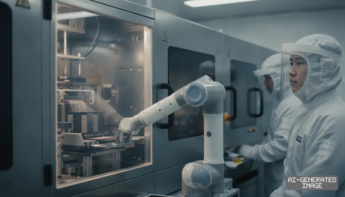
Samsung Electronics opened its next-generation HBM4 custom base die supply to rival foundry TSMC on Sept. 16, 2026, establishing a dual-track manufacturing model to secure artificial intelligence chip orders.
The shift allows AI accelerator designers to pair Samsung DRAM with Taiwan Semiconductor Manufacturing Co. logic dies. High-bandwidth memory chips are projected to account for over 60% of total HBM revenue late this year.
Samsung began commercial mass production of standard HBM4 on Feb. 12, 2026, integrating sixth-generation 10nm-class DRAM onto its internal 4nm logic base die. The company held a 33% share of global HBM shipments in the second quarter.
TSMC commands more than 50% of worldwide foundry capacity and manufactures custom accelerator silicon for Nvidia. Under the dual-track system, customers desiring TSMC packaging can select Taiwanese wafer lines for the bottom logic die.
A base die — the underlying logic layer that routes electric signals between stacked memory and processors — coordinates high-speed transmission. Custom HBM architectures require closer physical integration with host graphics processing units than earlier memory stacks needed.
Samsung's memory division will direct chip architecture for orders routed to TSMC wafer lines, industry participants said. Its internal System LSI design unit will focus exclusively on packages produced in Samsung foundries.
Rival chipmaker SK hynix already relies on TSMC logic lines for its sixth-generation HBM4 production. SK hynix captured roughly 53% of the overall HBM market during the previous product cycle, according to industry trackers.
The collaborative framework builds on initial technical work revealed two years ago. TSMC Ecosystem and Alliance Management head Dan Kochpatcharin announced in Taipei on Sept. 5, 2024 that the two rivals were co-developing bufferless HBM4.
A bufferless design removes intermediate distribution circuitry to reduce power consumption and decrease operational latency. That configuration permits memory dies to communicate directly with computing processors, cutting power draw by an estimated 40%, engineers said.
Former Samsung memory chief Lee Jung-bae said in September 2024 that the firm was preparing more than 20 customized solutions with external foundries. The current operational structure turns those early engineering consultations into client manufacturing choices.
Samsung previously emphasized a single-firm turnkey model, marketing proprietary DRAM, internal foundry fabrication and in-house packaging together. Major cloud providers and accelerator developers, however, requested foundry flexibility to match TSMC advanced packaging production lines, industry sources said.
Nvidia designs specialized accelerators under its proprietary NVHBM specifications that favor TSMC packaging infrastructure. Fabricating the base die on TSMC wafer lines reduces mechanical alignment risks during final chip-on-wafer assembly, packaging engineers said.
Samsung Foundry has achieved 4nm production yields exceeding 80%, closing performance gaps with international rivals. Retaining internal 4nm capacity allows the company to serve clients seeking single-vendor pricing and shorter supply routes, analysts said.
The dual-track model also permits Samsung to allocate cleanroom resources between high-margin AI stacks and commodity products. Samsung has evaluated transferring standard DDR5 module assembly to external test and packaging vendors to clear fab space, industry sources said.
Competitor Micron Technology unveiled 512GB DDR5 modules while pursuing its own HBM4 development roadmap. The parallel moves reflect an industry transition where memory makers assemble specialized supply consortia rather than relying on fully isolated manufacturing loops.
Samsung scheduled initial engineering sample deliveries of the TSMC-compatible custom HBM4 configurations for 2027. Commercial volume allocations will depend on client qualification rounds conducted across next year, according to supply chain participants.
Regulatory filings on the Korea Exchange do not confirm binding wafer procurement volumes or signed customer supply agreements as of Sept. 16, 2026. Neither Samsung nor TSMC has published contract pricing schedules.
Samsung Foundry continues operating its proprietary 4nm production line in Pyeongtaek, South Korea, while memory engineers complete validation routines for customer-specified base die layouts, according to company production schedules.
Impact map
How this development propagates across the region and out to global buyers.
| Event | Korea | China | Japan | Global impact |
|---|---|---|---|---|
| custom HBM4 base die dual-track | Samsung captures packaging-flexible AI orders while SK hynix faces tighter foundry allocation | domestic AI chipmakers face delayed access to TSMC-packaged high-density HBM4 | Tokyo Electron and packaging chemical suppliers see steady tool and resin demand across both foundry routes | AI accelerator makers gain dual-sourced HBM4 base die supply and lower supply disruption risk |
In this story
- Companies
- Samsung ElectronicsTaiwan Semiconductor Manufacturing Co.
- Tickers
- 005930.KS2330.TW
- Exposed
- NvidiaSK hynixMicron Technology
- Policy
- Economic SecuritySubsidies
- Impact
- Supply ChainCapexOrder Book
Track every Economic Security development → Track every Subsidies development →
Related briefings
- SK hynix starts $4 billion packaging plant in Indiana to feed US AI Also on Micron Technology, Nvidia, SK hynix
- Samsung narrows SK hynix HBM lead as HBM4 shipments expand Also on Micron Technology, Nvidia, SK hynix
- DeepSeek cuts AI memory use 75%, rattling global chipmakers Also on Micron Technology, Nvidia, SK hynix
- TSMC Urges HBM Makers to Adopt X-Ray Friendly Chip Design for Advanced Packaging Also on Micron Technology, Nvidia, SK hynix
Sources
Reporting
Confidence: medium — how we grade this
The documents behind this briefing are linked above. East Asia Brief produces its English text with AI assistance under human editorial review, and does not translate or republish other outlets' articles. See our methodology and AI policy. Spotted an error? Tell us.
The Morning Brief
What changed in Korean, Chinese and Japanese industry overnight — and what it means for your supply chain. One email, weekday mornings, US time. Free.
The first issue goes out shortly. Sign up now and you will not miss it.