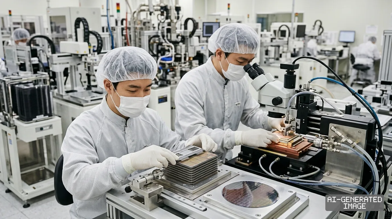
Micron unveils vertical HBM architecture to stack on AI GPUs
The US chipmaker outlines direct 3D memory-on-logic packaging using hybrid copper bonding to eliminate interposers, challenging packaging architectures from SK hynix and Samsung.
Micron Technology unveiled a roadmap on Oct. 22, 2026, to vertically stack high-bandwidth memory directly onto artificial intelligence processors, bypassing silicon interposers to eliminate interconnect data bottlenecks.
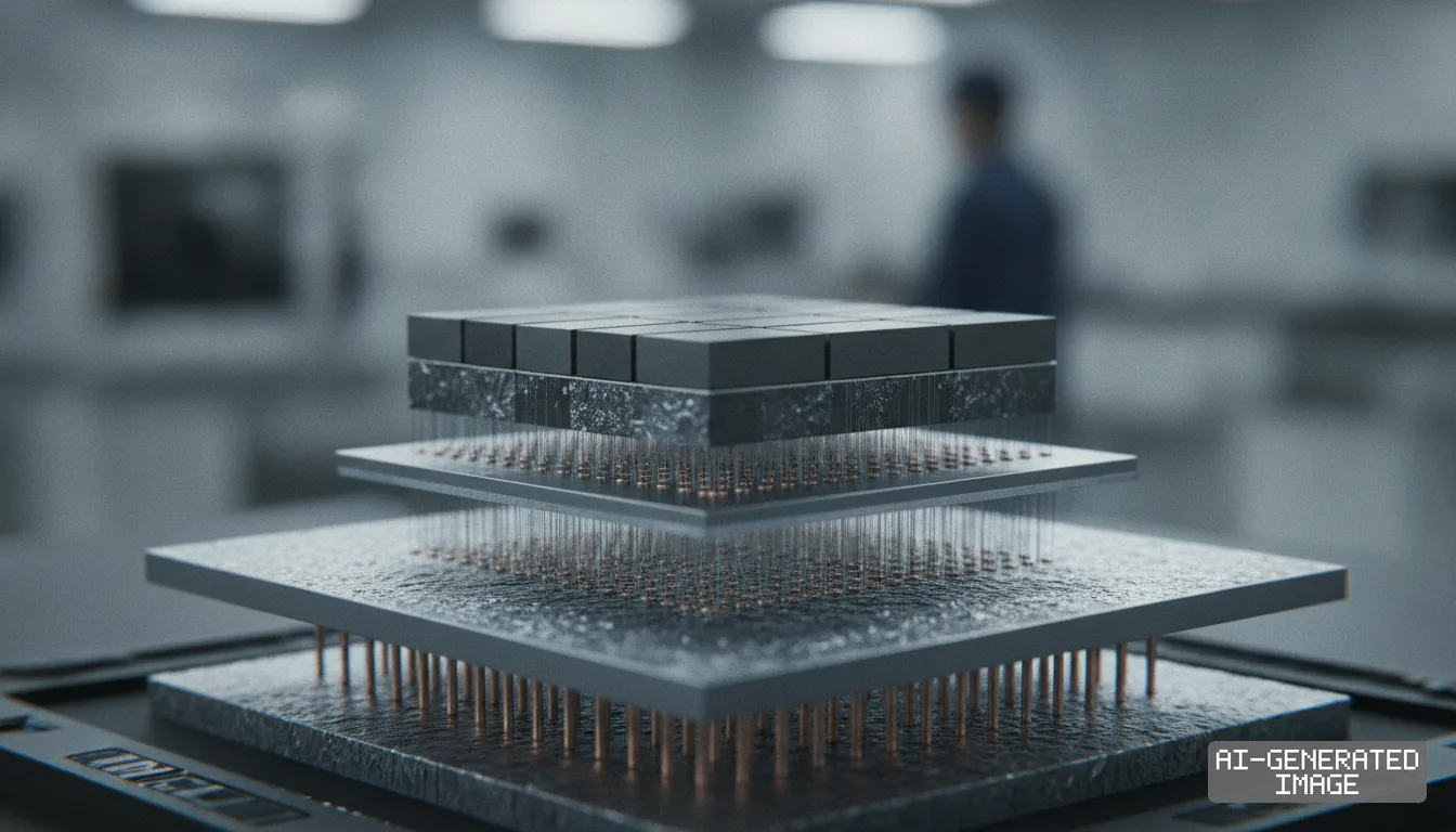
The architecture, designated vertical high-bandwidth memory, places dynamic random-access memory dies directly over host compute logic. The direct physical interface shortens data transit distance and lowers signal resistance.
The company currently manufactures 12-high 36-gigabyte HBM4 modules operating above 2.8 terabytes per second. That product accounts for roughly 10% of current global shipments for advanced artificial intelligence accelerators.
Artificial intelligence workloads require higher bandwidth and lower power per token, Scott DeBoer said. DeBoer serves as president and chief technology and products officer at the Boise, Idaho-based semiconductor maker.
Standard 2.5D packaging positions memory stacks beside compute processors on a silicon interposer. Horizontal trace lines across the interposer introduce capacitive load and thermal resistance as accelerators demand more throughput.
Direct vertical stacking eliminates the interposer by attaching memory directly to the processor surface. The layout yields higher bandwidth per watt by compressing the physical communication path into vertical microscopic channels.
Connecting the silicon layers requires bumpless hybrid copper bonding, Micron said. The technique bonds copper-to-copper contacts and dielectric material simultaneously, reducing connection pitch below the physical threshold of traditional microbumps.
Vertical integration concentrates thermal energy directly beneath the memory layers. Micron developed an integrated chimney heat spreader positioned over the physical layer of the base die to draw heat upward and outward.
The company scheduled commercial volume manufacturing of its first-generation vertical architecture for 2028. A third-generation version, known as vHBM3, is slated for high-volume manufacturing around 2030.
Micron also introduced vertical edge inference memory for decentralized artificial intelligence systems. The component targets bandwidth of two terabytes per second and power efficiency below one picojoule per bit starting in 2028.
Vertical architectures will not immediately replace traditional modules, the company said. Standard 2.5D HBM packaging will coexist with vertically stacked solutions across enterprise data centers through the end of the decade.
Micron began volume shipments of 12-high HBM4 memory in March 2026 for Nvidia's Vera Rubin computing platform. The memory supplier is sampling 16-high 48-gigabyte modules and next-generation HBM4E units to primary customers.
High-bandwidth memory procurement has shifted toward bespoke engineering, DeBoer said. Memory suppliers must now build custom logic base dies tailored to proprietary accelerator architectures, moving beyond standard industry baselines.
DeBoer also rejected the 4F² DRAM cell structure promoted by ChangXin Memory Technologies. The Hefei-based Chinese memory producer disclosed plans to market server-grade DDR5 memory modules using 4F² architectures by late 2026.
Micron studied 4F² structures for 20 years before abandoning the design, DeBoer said. High process complexity, strict alignment tolerances and the floating body effect — where trapped electrical charge causes voltage instability — degrade production yields.
Bit density depends on capacitor pitch rather than interconnect transistor layout, the company said. Micron plans to maintain 6F² planar DRAM manufacturing through 2030 before transitioning directly to true three-dimensional DRAM.
The chipmaker currently operates its 1-gamma DRAM manufacturing node at high volume. Its next-generation 1-delta node enters volume production in the second half of 2027, delivering a mid-20% density gain.
Micron also presented manufacturing targets for its 11th-generation NAND flash memory. The design stacks more than 400 active word-line layers using wafer-on-wafer bonding, with mass production scheduled for late 2027.
The vertical packaging roadmap escalates competition with South Korean memory makers. Samsung Electronics revealed a similar vertical stacking concept called zHBM in August 2026, relying on its internal contract foundry to bundle manufacturing.
SK hynix holds over 50% market share in high-bandwidth memory for artificial intelligence servers. The supplier is developing proprietary 3D packaging technologies to protect its lead in Nvidia accelerator supply chains.
Direct vertical stacking shifts packaging value away from traditional contract foundries. Memory suppliers must now master logic integration, challenging advanced packaging workflows operated by Taiwan Semiconductor Manufacturing Co.
Commercial deployment begins with vHBM1 scheduled for high-volume manufacturing in 2028, following the production ramp of 1-delta DRAM in the second half of 2027.
The presentation slides do not state which foundry partner will fabricate the custom logic base dies, and Micron has not named the lead cloud customer for vHBM1.
Impact map
How this development propagates across the region and out to global buyers.
| Event | Korea | China | Japan | Global impact |
|---|---|---|---|---|
| Direct vertical HBM architecture | SK hynix and Samsung face direct architecture challenge to 2.5D HBM packaging where they hold over 85% share | CXMT 4F² DRAM rejected by global suppliers, preserving technical barriers in server DDR5 | Equipment makers see expanded order books for hybrid bonding and wafer bonding tools | GPU accelerators bypass silicon interposers, shifting packaging value away from pure-play foundries |
In this story
- Companies
- Micron Technology
- Tickers
- MU
- Exposed
- SK hynixSamsung ElectronicsNvidiaTaiwan Semiconductor Manufacturing CoChangXin Memory Technologies
- Impact
- CapexSupply ChainPricing
Related briefings
- Micron Cuts DRAM Lead of SK hynix to One Point on HBM Demand Also on ChangXin Memory Technologies, Micron Technology, Nvidia
- CXMT lifts revenue sixfold to 119.7 billion yuan on memory volume push Also on ChangXin Memory Technologies, Micron Technology, SK hynix
- CXMT plans 4F² server DRAM launch, hitting memory shares Also on ChangXin Memory Technologies, Micron Technology, SK hynix
- CXMT starts 5th-gen DRAM output, bypassing US tool controls Also on ChangXin Memory Technologies, Micron Technology, SK hynix
Sources
Primary documents
Reporting
Confidence: high — how we grade this
The documents behind this briefing are linked above. East Asia Brief produces its English text with AI assistance under human editorial review, and does not translate or republish other outlets' articles. See our methodology and AI policy. Spotted an error? Tell us.
The Morning Brief
What changed in Korean, Chinese and Japanese industry overnight — and what it means for your supply chain. One email, weekday mornings, US time. Free.
The Morning Brief is in preparation. Leave your address and we will write to you once — when the first issue is ready. Nothing before that.