Shinko buys Japan Display plant to build advanced packaging hub
The 373,483-square-meter Mobara factory will yield a 51.4 billion yen gain for JDI while giving Shinko flip-chip substrate capacity for artificial intelligence processors.
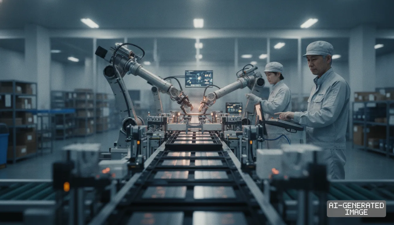
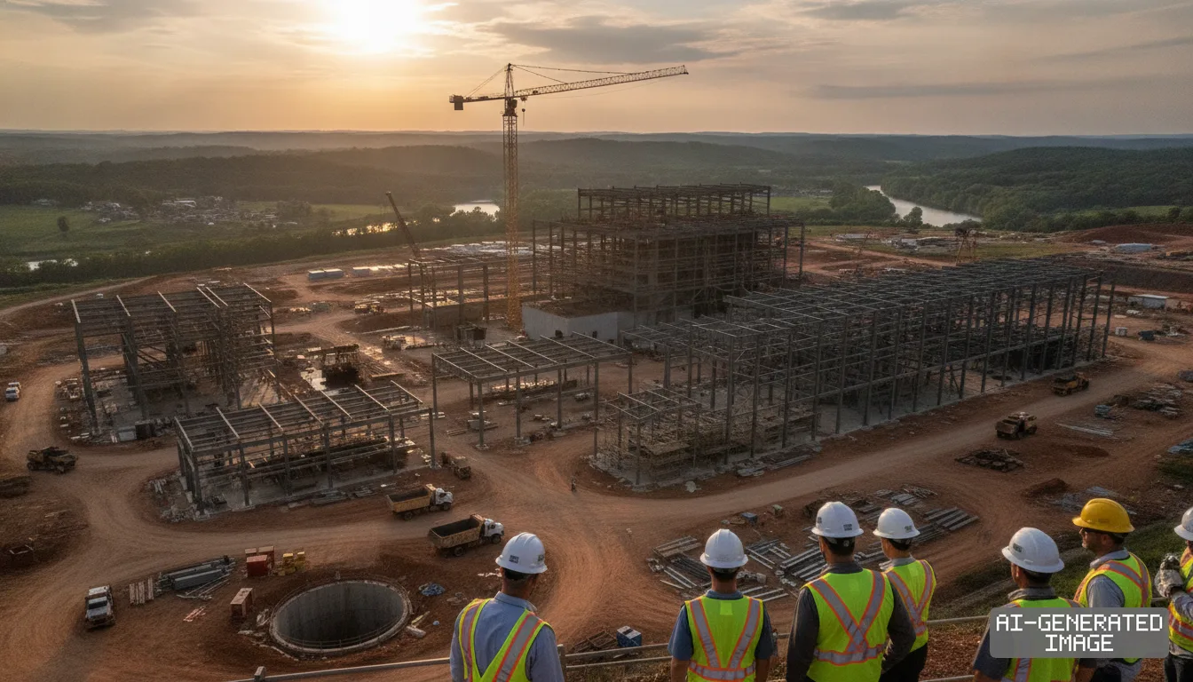
Japan Display Inc. and Shinko Electric Industries detailed handover terms on Oct. 11, 2026 to repurpose JDI's 373,483-square-meter Mobara factory into an advanced artificial intelligence semiconductor packaging substrate hub.
The transaction transfers Japan Display's former flagship liquid crystal display facility in Chiba Prefecture. JDI expects to record a 51.4 billion yen ($325 million) extraordinary gain on the transfer against a book value of 26.6 billion yen.
The divestment represents the largest structural asset sale in the restructuring drive at JDI, which had booked 12 consecutive annual net losses through March 2026. That deficit pushed company equity to a negative net worth of 7.4 billion yen.
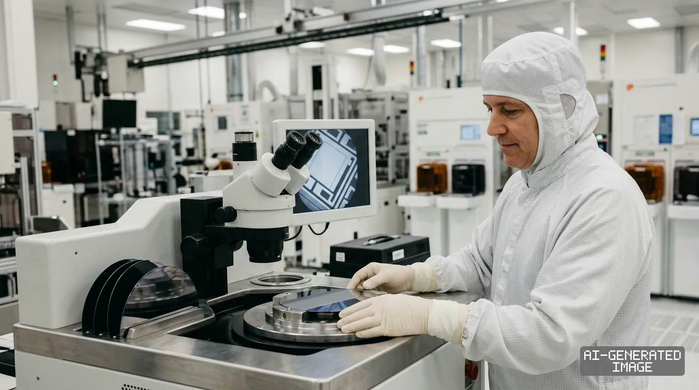
Shinko manufactures integrated circuit substrates and leadframes. The company provides flip-chip ball grid array packages — multilayer resin foundations that route high-density electrical signals between silicon dies and system boards — to major graphic processor designers.
Surging hardware demand for artificial intelligence accelerators has overwhelmed global packaging lines. Accelerators combine multiple logic dies with high bandwidth memory on wide footprints.
Those silicon assemblies demand larger substrate areas with tighter line spacing. Traditional printed circuit board plants cannot match the micron-level tolerance needed for interposer connections.
Display fabrication plants offer an immediate physical substitute. Liquid crystal lines contain vibration-damped concrete flooring, high-volume ultrapure water supply networks and industrial electrical substations.
They also feature extensive Class 100 cleanrooms — sealed production spaces where air filtration limits airborne contaminants to under 100 particles per cubic foot. Building an equivalent greenfield packaging fab requires four to five years.
Converting an established flat-panel display campus reduces construction timelines by roughly two years, engineering managers said. Shinko plans to begin commercial operations at the renovated Mobara site during fiscal 2028.
The site allocation divides the Mobara property between two manufacturing partners. Shinko will retain the eastern zone of roughly 140,738 square meters for its own advanced flip-chip package production.
Shinko agreed to transfer the western area of 232,745 square meters — representing 62% of the total property — to partner manufacturer FICT Co., Ltd.. FICT builds high-density multi-layer printed wiring boards.
The combined campus establishes an integrated domestic hub for backend semiconductor components. Both firms plan to link engineering workflows across substrate cores and assembly stages.
Panel manufacturing at Mobara ceased in November 2025. JDI had operated Generation 6 glass processing lines at the site, producing small panels for Apple Inc. smartphones and Apple Watch displays.
The manufacturer shuttered those lines after consumer electronics makers shifted display procurement toward organic light-emitting diode panels from South Korea and China.
The closure left JDI with heavy fixed depreciation charges. Selling the Mobara plant leaves the company with a single domestic manufacturing asset at Ishikawa, which fabricates specialized automotive and industrial displays.
JDI has pivoted toward an asset-light licensing model for eLEAP, its proprietary photolithography OLED process. The company is also redirecting research staff toward glass-based semiconductor interposers.
The Mobara transaction reflects a broader realignment across Japan's electronics manufacturing base. Japanese flat-panel producers are transferring idle infrastructure to semiconductor manufacturers racing to clear packaging bottlenecks.
Sharp Corporation signed a comparable agreement with back-end specialist Aoi Electronics Co., Ltd. to convert 60,000 square meters of floor space at its Mie Plant No. 1.
Aoi Electronics is installing production lines at the Mie site to manufacture 20,000 panel-level packages per month by 2026. The lines process fan-out laminate packaging on large rectangular glass carriers.
Using rectangular display glass instead of 300-millimeter circular silicon wafers sharply increases substrate surface area. Rectangular panels yield more usable units per batch with minimal edge waste.
Dai Nippon Printing and Resonac Holdings have formed industry consortiums to establish standard glass-core substrate production lines across Japan. Glass cores avoid the heat-induced warpage common in organic substrates under thermal stress.
JDI and Shinko scheduled the physical handover of the Mobara site for March 31, 2027. That date permits JDI to clear residual processing gear and book its 51.4 billion yen gain in the fiscal year ending March 2027.
The companies did not disclose the total purchase price, and Shinko has not published the capital expenditure budget allocated for cleanroom retooling.
Impact map
How this development propagates across the region and out to global buyers.
| Event | Korea | China | Japan | Global impact |
|---|---|---|---|---|
| Japan display fab conversion to packaging | Packaging subcontractors face future Japanese glass-substrate competition | Display panel dominance consolidates as Japanese legacy fabs exit LCD lines entirely | Shinko and FICT gain 373,483 square meters of ready cleanroom capacity in Chiba | AI server supply chains secure secondary non-wafer substrate capacity for high-density accelerators |
In this story
- Companies
- Japan Display Inc.Shinko Electric Industries
- Tickers
- 6740.T6967.T
- Exposed
- FICTSharp CorporationAoi ElectronicsApple
- Policy
- Economic SecuritySubsidies
- Impact
- Supply ChainCapexCost Structure
Track every Economic Security development → Track every Subsidies development →
Related briefings
- Japan Display sells Mobara fab to Shinko for chip packaging Also on Japan Display Inc., FICT, Shinko Electric Industries
- Ibiden and Shinko ramp high-layer FC-BGA lines as AI server package sizes expand Also on Shinko Electric Industries, Cost Structure
- South Korean substrate makers develop embedded silicon bridges for AI chips Also on Shinko Electric Industries, Cost Structure
- TSMC plans to lift wafer foundry prices by 3% to 6% from 2027 Also on Apple, Cost Structure
Sources
Reporting
Confidence: medium — how we grade this
The documents behind this briefing are linked above. East Asia Brief produces its English text with AI assistance under human editorial review, and does not translate or republish other outlets' articles. See our methodology and AI policy. Spotted an error? Tell us.
The Morning Brief
What changed in Korean, Chinese and Japanese industry overnight — and what it means for your supply chain. One email, weekday mornings, US time. Free.
The Morning Brief is in preparation. Leave your address and we will write to you once — when the first issue is ready. Nothing before that.