HANMI Semiconductor expands San Jose hub for HBM chip bonders
The bonder maker invested $1.5 million in a California unit after a 90.8 billion won quarterly profit, targeting packaging plants at Micron and SK hynix.
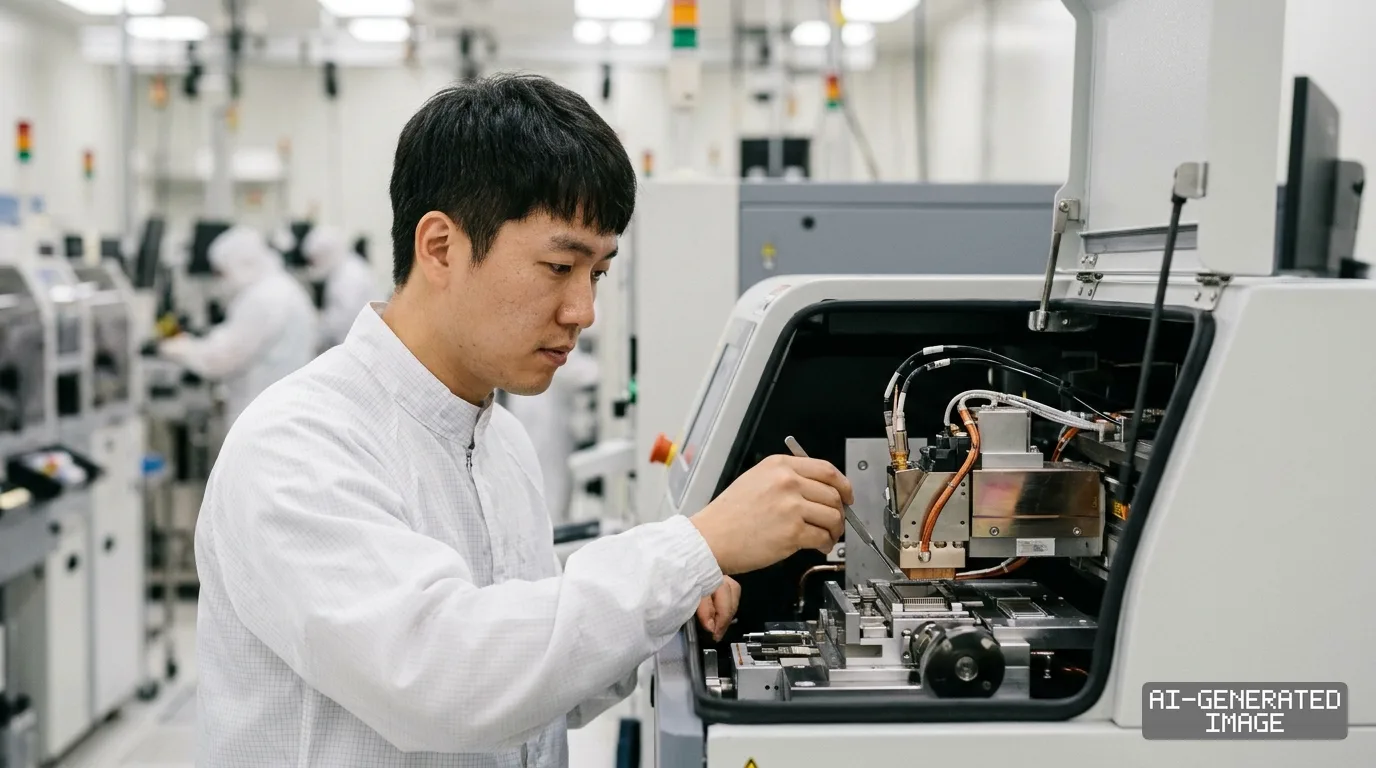
HANMI Semiconductor outlined plans on Nov. 6, 2026, to expand field engineering deployments across North America following the launch of its California subsidiary, targeting packaging lines at major chipmakers.
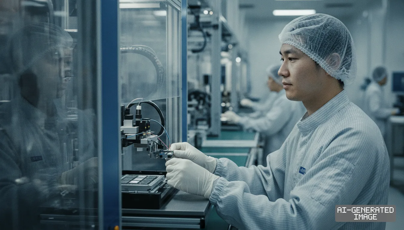
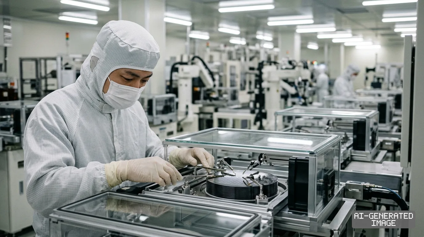
The South Korean equipment maker designs thermo-compression bonders — thermal tools that join memory dies with heat and pressure — used to assemble high-bandwidth memory for artificial intelligence accelerators.
HANMI Semiconductor invested $1.5 million to establish Hanmi USA Inc. in San Jose, supporting tools where the company held an estimated 71.2% global market share in high-bandwidth memory bonding last year.
The initial equity investment accounts for a 100% stake in the California operating entity, according to corporate registration filings submitted to the Korea Exchange.
Preliminary third-quarter financial figures released Oct. 30 showed operating profit reached 90.8 billion won ($65.8 million) on revenue of 181.0 billion won, producing an operating margin of 50.2%.
Demand for advanced packaging equipment has expanded as commercial semiconductor manufacturers build new fabrication sites across the United States with funding allocated under the CHIPS and Science Act.
Micron Technology awarded HANMI Semiconductor a 22.6 billion won ($16.4 million) purchase order for Dual TC Bonder Tiger equipment, booking tool shipments for American production sites.
Micron plans to introduce commercial high-bandwidth memory fabrication at its facility in Boise, Idaho in 2027, followed by a $100 billion megafab complex in Clay, New York.
SK hynix broke ground in August on a $3.87 billion advanced packaging plant in West Lafayette, Indiana, intending to package high-bandwidth memory stacks for North American artificial intelligence customers.
Intel launched manufacturing on its 18A process node alongside advanced packaging lines at Chandler, Arizona in late 2025, lifting domestic requirements for cleanroom equipment installation and calibration services.
Amkor Technology expanded planned capital investment to $12 billion for its packaging campus in Peoria, Arizona, creating the first large-scale outsourced semiconductor assembly and test facility in the United States.
HANMI Semiconductor stations skilled field engineers at the San Jose operational base to provide rapid on-site maintenance, cutting tool-calibration downtime as American client factories install advanced packaging lines.
The California unit represents the equipment maker's fourth international operational branch, adding an American engineering office alongside existing subsidiary locations in Taiwan, mainland China and Singapore.
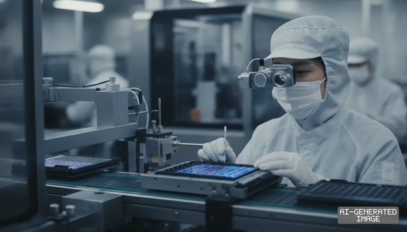
Beyond vertical memory stacking machinery, HANMI Semiconductor shipped its FC Bonder 75 equipment to a Taiwanese foundry customer in September, expanding shipments into 2.5-dimensional packaging for graphics processing units.
The 2.5-dimensional tool connects logic processors directly with surrounding high-bandwidth memory dies on large silicon interposers — thin wiring bases that route electrical signals between adjoining silicon chips.
Samsung Electro-Mechanics awarded HANMI Semiconductor a 24.5 billion won supply agreement in October for micro SAW and vision placement tools, which slice, inspect, sort and stack printed circuit substrates.
The equipment manufacturer maintains global dominance in micro SAW systems, holding the leading market position worldwide across back-end cutting and sorting equipment for discrete semiconductor components.
The establishment of Hanmi USA marks the company's first operational facility in the United States since its founding in Incheon 46 years ago in 1980.
Late founder Kwak No-gwon spent 14 years working at Motorola starting in 1967 before founding HANMI Semiconductor in South Korea with technical assistance from the American electronics producer.
The corporate name reflects the late founder's objective to link South Korean and American semiconductor supply chains, according to company statements released at the Silicon Valley facility launch.
Chairman Kwak Dong-shin first disclosed the American expansion strategy on May 15 at the company's Incheon headquarters, citing direct technical coordination with Silicon Valley cloud service providers.
Hyperscale data center operators such as Alphabet, Microsoft, Amazon Web Services and Meta increasingly specify packaging parameters directly to hardware suppliers while developing proprietary artificial intelligence accelerators.
Executive leadership held a formal opening ceremony at the San Jose office on Oct. 16, formally incorporating the business unit four days later on Oct. 20, the company said.
Operating schedules show volume commercial packaging runs at Amkor's Peoria site and SK hynix's West Lafayette facility will commence operations in 2028, setting deployment milestones for California engineers.
Micron targets volume delivery of next-generation memory dies from its Boise fab in 2027, establishing an intermediate integration deadline for tooling support teams stationed in California.
The manufacturer operates an integrated production structure at its Incheon headquarters, handling metal casting, mechanical processing, software design and final cleanroom assembly internally across 340 global customer relationships.
Domestic manufacturing facilities in Incheon continue fabricating Dual TC Bonder tools for export, while the San Jose subsidiary focuses on cleanroom field integration, emergency repairs and customer modifications.
Regulatory filings do not disclose the precise engineering headcount assigned to the San Jose facility, and the company has not published service fee structures for North American tool maintenance.
Nomura Securities hosted an institutional investor conference call on Nov. 6, reviewing third-quarter operating performance and global packaging tool deliveries with international asset management firms.
Impact map
How this development propagates across the region and out to global buyers.
| Event | Korea | China | Japan | Global impact |
|---|---|---|---|---|
| US advanced packaging tool support | HANMI Semiconductor secures direct cleanroom access across US fab construction projects | Domestic memory assemblers lose access to premier TC bonder field maintenance | Tool suppliers encounter intensified packaging competition at North American logic lines | Foundries and memory makers shorten advanced packaging ramp cycles in the United States |
| US advanced packaging tool support | HANMI Semiconductor secures direct cleanroom access across US fab construction projects | Domestic memory assemblers lose access to premier TC bonder field maintenance | Tool suppliers encounter intensified packaging competition at North American logic lines | Foundries and memory makers shorten advanced packaging ramp cycles in the United States |
In this story
- Companies
- HANMI Semiconductor
- Tickers
- 042700.KS
- Exposed
- Micron TechnologySK hynixIntelAmkor TechnologySamsung Electro-Mechanics
- Impact
- Supply ChainCapexOrder Book
Related briefings
- Hanmi Semiconductor opens US office for AI memory packaging Also on Hanmi Semiconductor, Amkor Technology, Micron Technology
- Hanmi Semiconductor cements 71% share in HBM TC bonder tools Also on Hanmi Semiconductor, Samsung Electro-Mechanics, Micron Technology
- Hanmi Semiconductor wins $18 million tool deal from Samsung Also on Hanmi Semiconductor, Samsung Electro-Mechanics, Micron Technology
- South Korean substrate makers develop embedded silicon bridges for AI chips Also on Amkor Technology, Samsung Electro-Mechanics, Intel
Sources
Primary documents
Reporting
Confidence: high — how we grade this
The documents behind this briefing are linked above. East Asia Brief produces its English text with AI assistance under human editorial review, and does not translate or republish other outlets' articles. See our methodology and AI policy. Spotted an error? Tell us.
The Morning Brief
What changed in Korean, Chinese and Japanese industry overnight — and what it means for your supply chain. One email, weekday mornings, US time. Free.
The Morning Brief is in preparation. Leave your address and we will write to you once — when the first issue is ready. Nothing before that.