Hanmi Semiconductor opens US office for AI memory packaging
The South Korean equipment maker committed $1.5 million to Hanmi USA in San Jose to support Micron and other memory customers building packaging fabs across North America.
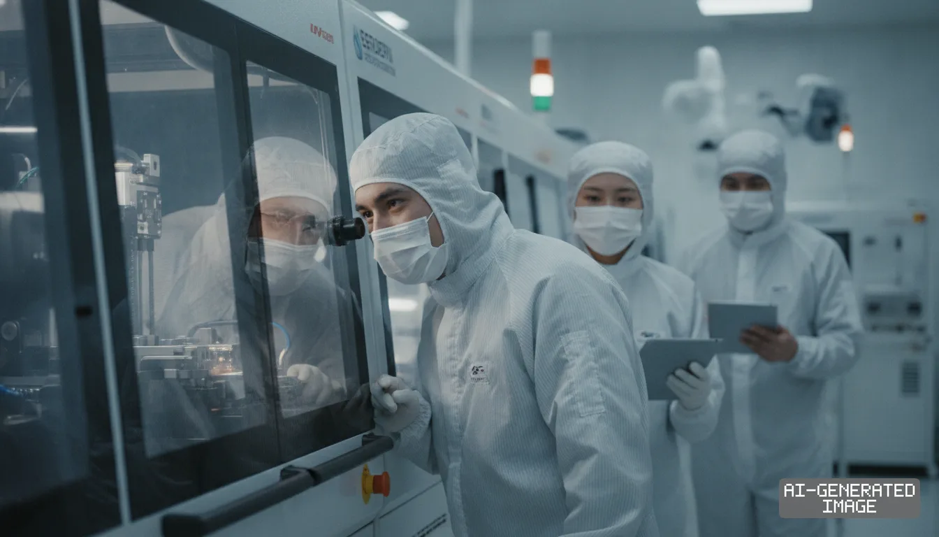
Hanmi Semiconductor established its United States subsidiary, Hanmi USA Inc., on Oct. 20, 2026, opening a San Jose facility to provide field engineering support for North American advanced packaging customers.
The South Korean equipment maker invested $1.5 million (about 2.1 billion won) to acquire a 100% equity stake in the California entity, according to a regulatory filing submitted to the Korea Exchange.
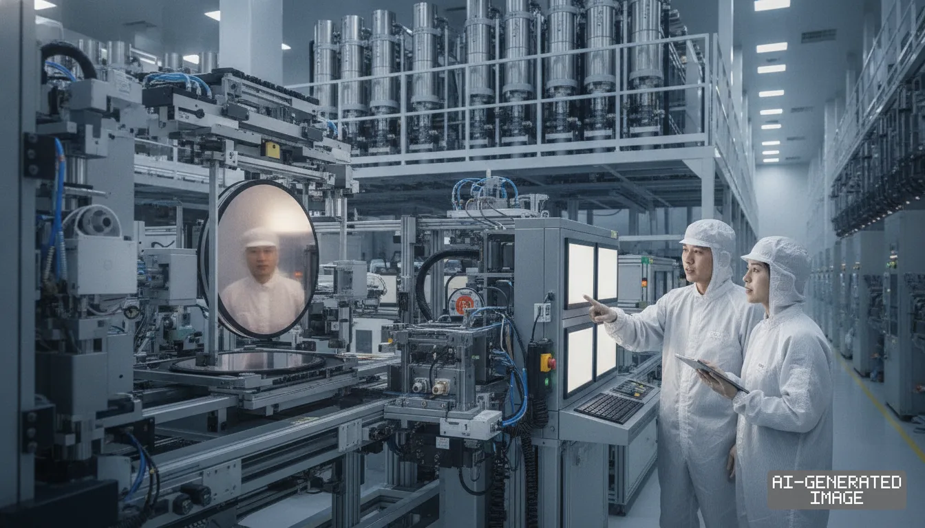
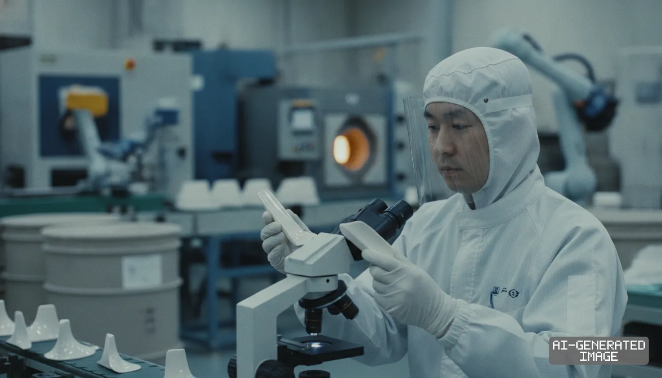
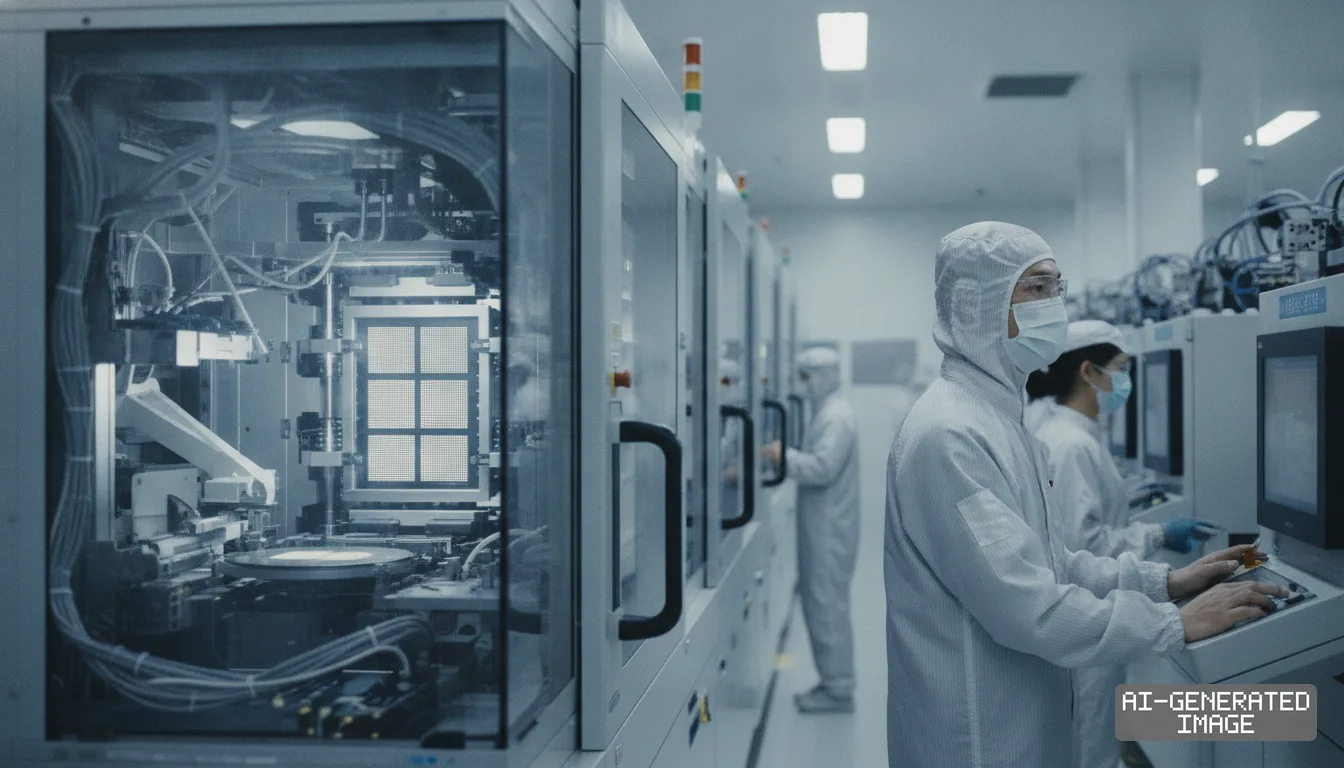
The company holds the top position in thermo-compression (TC) bonders — thermal equipment that joins memory dies with heat and pressure — accounting for the majority of tools used in high-bandwidth memory (HBM) stacking.
The new subsidiary represents the equipment maker's fourth overseas branch, adding an American presence alongside existing operating hubs in Taiwan, China and Singapore, the company said.
San Jose will serve as an integrated operational command center for field engineers dispatched to fab sites across North America, according to the company announcement.
Hanmi Semiconductor founded its business in 1980 under a corporate name chosen by late founder Kwak Noh-kwon, who intended the firm to bridge South Korean and American semiconductor supply chains.
The expansion follows capital expenditure across the United States encouraged by subsidies under the CHIPS and Science Act, which attracted new fabrication and packaging facilities from memory and logic manufacturers.
Micron Technology awarded Hanmi a 22.6 billion won ($16.4 million) contract for Dual TC Bonder Tiger equipment, and plans to bring new memory lines online in Boise, Idaho.
The American memory producer aims to start volume manufacturing of high-bandwidth memory at the Boise facility in 2027, followed by a $100 billion megafab project in Clay, New York.
SK hynix broke ground in August on a $3.87 billion advanced packaging facility in West Lafayette, Indiana, where it plans to package next-generation memory for artificial intelligence accelerators.
Commercial wafer stacking at the West Lafayette packaging plant will begin in the second half of 2028, requiring dedicated tooling maintenance and process recipe adjustments on site.
Contract packager Amkor Technology increased its planned capital expenditure for a packaging campus in Peoria, Arizona, to $12 billion, scheduling initial cleanroom operations for early 2028.
The Peoria site marks the first large-scale outsourced assembly and test facility constructed on American soil, offering advanced multi-die packaging to domestic chip designers, the company said.
Intel began operating its 18A process node alongside proprietary advanced packaging lines in Chandler, Arizona, lifting domestic American demand for high-precision die-bonding machinery and defect inspection systems.
Hanmi supplies micro saw and vision placement equipment, automated machinery that slices, cleans, inspects and sorts processed silicon wafers, holding the leading global market share in the segment.
The equipment maker broadened its catalog beyond memory stacking by releasing 2.5D packaging bonders and flip-chip bonders designed to connect logic dies directly to silicon interposers.
Hanmi developed the Dual TC Bonder Tiger alongside its Griffin and Dragon tool lines to accommodate differing substrate specifications requested by international memory fabricators.
The equipment manufacturer established a dedicated intellectual property department in 2002 and has filed more than 110 patent applications protecting proprietary mechanisms used in its memory bonding machines.
Hanmi shipped its FC Bonder 75 tool to an international customer in September, followed by a 24.5 billion won ($17.8 million) order for wafer-sawing equipment from Samsung Electro-Mechanics.
Development of mild hybrid bonding tools for sixth-generation HBM4 production began earlier to prepare for stacking architectures scheduled for commercial delivery before 2029.
Locating application engineers in California reduces equipment downtime for chipmakers running complex bonding cycles that require precise thermal calibration and mechanical alignment during initial fab ramp-ups.
Equipment rival ASMPT, based in Singapore, manufactures its assembly tools at production facilities in Shenzhen and Chengdu in China, facing logistical hurdles when supporting American semiconductor lines.
Direct engineering coverage gives Korean suppliers a competitive advantage as memory makers test tighter tolerances for 12-layer and 16-layer memory stacks used in advanced AI clusters.
Chairman Kwak Dong-shin said in August that establishing the American base would allow the equipment maker to capture orders from emerging megafabs and domestic AI semiconductor alliances.
Hanmi Semiconductor generated record quarterly revenue of 208.5 billion won ($151 million) and operating profit of 99.3 billion won in the third quarter of 2024 on booming bonder shipments.
The regulatory filing does not state how many technical service engineers will be permanently stationed at the San Jose office during its initial operating phase.
Hanmi USA will coordinate tool deliveries and site acceptance testing as Micron and SK hynix install cleanroom equipment across their respective American construction sites throughout 2027.
Impact map
How this development propagates across the region and out to global buyers.
| Event | Korea | China | Japan | Global impact |
|---|---|---|---|---|
| Hanmi launches Hanmi USA | Hanmi secures direct US service hub, shielding SK hynix packaging supply chain | Rival ASMPT faces disadvantage serving US fabs from Shenzhen plants | Tokyo Electron packaging tools face closer Korean on-site integration in US | US packaging timelines for Micron and Amkor gain dedicated vendor tooling support |
| Hanmi launches Hanmi USA | Hanmi secures direct US service hub, shielding SK hynix packaging supply chain | Rival ASMPT faces disadvantage serving US fabs from Shenzhen plants | Tokyo Electron packaging tools face closer Korean on-site integration in US | US packaging timelines for Micron and Amkor gain dedicated vendor tooling support |
In this story
- Companies
- Hanmi Semiconductor
- Tickers
- 042700.KS
- Exposed
- Micron TechnologySK hynixAmkor Technology
- Policy
- Subsidies
- Impact
- CapexSupply Chain
Track every Subsidies development →
Related briefings
- Hanmi Semiconductor Wins Tool Order for Musk's Terafab Plant Also on Hanmi Semiconductor, Micron Technology, SK hynix
- Hanmi Semiconductor wins $18 million tool deal from Samsung Also on Hanmi Semiconductor, Micron Technology, SK hynix
- South Korea funds advanced chip packaging and backside power pilot lines Also on Hanmi Semiconductor, SK hynix, Subsidies
- SK hynix delays HBM4 equipment procurement into early 2027 Also on Hanmi Semiconductor, SK hynix
Sources
Primary documents
Reporting
Confidence: high — how we grade this
The documents behind this briefing are linked above. East Asia Brief produces its English text with AI assistance under human editorial review, and does not translate or republish other outlets' articles. See our methodology and AI policy. Spotted an error? Tell us.
The Morning Brief
What changed in Korean, Chinese and Japanese industry overnight — and what it means for your supply chain. One email, weekday mornings, US time. Free.
The Morning Brief is in preparation. Leave your address and we will write to you once — when the first issue is ready. Nothing before that.