GlobalFoundries signs $2B TSMC packaging deal for AI chips
The five-year agreement will produce silicon interposers at the Malta fab in New York starting in 2028 to ease CoWoS bottlenecks for artificial intelligence processors.
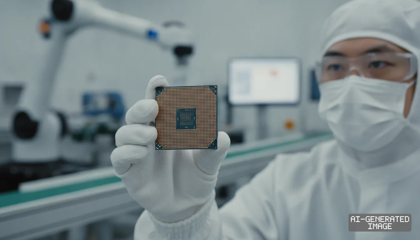
GlobalFoundries formalized a $2 billion manufacturing agreement with TSMC on Oct. 12 to supply silicon interposers for advanced artificial intelligence packaging across an initial five-year production contract.
The contract represents roughly 6% of annual revenue for GlobalFoundries when distributed across the five-year schedule. The company generated $6.79 billion in total revenue during 2025, according to its annual financial disclosures.
GlobalFoundries will expand manufacturing capacity at its Fab 8 facility in Malta, New York. The site will produce silicon interposers to support TSMC's proprietary Chip-on-Wafer-on-Substrate packaging platform, known commercially as CoWoS.
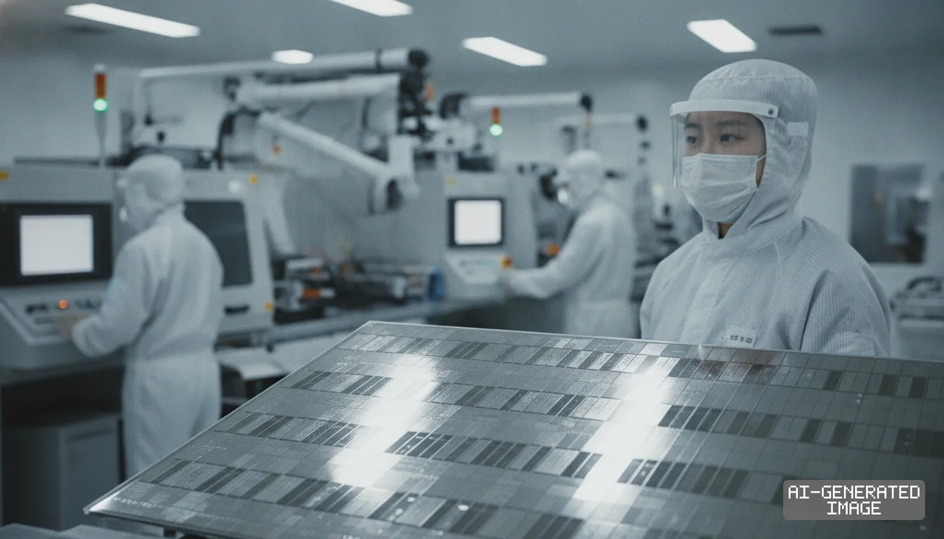
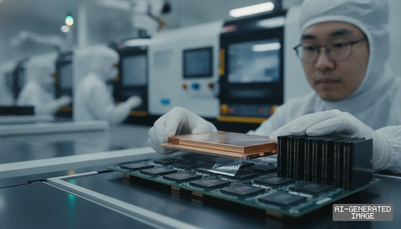
Silicon interposers are thin silicon slices that sit beneath processing dies and memory stacks. They provide high-density microscopic wiring that carries data between graphics processing units and high-bandwidth memory chips.
Advanced packaging has become the principal manufacturing bottleneck for artificial intelligence accelerators. Leading cloud computing operators have faced long delivery delays because packaging facilities could not match wafer production rates.
TSMC has expanded its packaging footprint in Taiwan to meet surging orders from Nvidia and other processor designers. The Taiwanese foundry plans to increase monthly packaging capacity from roughly 35,000 wafers to more than 130,000 wafers.
Producing passive silicon interposers consumes fab floor space that TSMC prefers to reserve for higher-margin logic manufacturing. Interposers rely on mature lithography nodes, primarily 65-nanometer patterning, rather than extreme ultraviolet equipment.
Subcontracting the interposer layer allows TSMC to expand packaging volume without tying up cleanroom bays in Taiwan. The arrangement keeps TSMC in control of the final multi-die assembly and testing stages.
GlobalFoundries brings specialized manufacturing capabilities derived from its acquisition of IBM's microelectronics unit in 2015. The Malta facility produces embedded deep trench capacitors, which are tiny energy-storage structures etched directly into silicon.
Those embedded capacitors stabilize power delivery inside complex artificial intelligence chips. As processor power consumption climbs beyond 1,000 watts, voltage fluctuations can degrade computing performance or damage silicon circuits.
Advanced packaging has become critical to delivering performance, power efficiency and scale for artificial intelligence systems, GlobalFoundries CMOS Business Senior Vice President Ed Kaste said.
Supplying these components from a domestic manufacturing base creates a secure source of packaging elements for industrial customers, Kaste said. The deal establishes the first domestic United States source for CoWoS interposers.
The agreement also aligns with federal industrial policy aimed at rebuilding domestic semiconductor production networks. The United States government has awarded billions of dollars in grants to onshore fabrication and advanced assembly.
TSMC is building three wafer fabrication facilities in Phoenix, Arizona, with planned investments reaching $65 billion. Securing domestic interposers helps TSMC construct a regional packaging supply chain for North American customers.
American chip design firms, including Nvidia, Apple and Advanced Micro Devices, currently ship completed silicon wafers from the United States back to Asian facilities for final packaging and integration.
Onshoring the interposer segment reduces transit risks across the Pacific Ocean. It also enables fabless designers to market processors as components manufactured and assembled inside the United States.
For GlobalFoundries, the contract provides steady baseload volume for mature 300-millimeter equipment at its New York campus. The company halted development of leading-edge 7-nanometer transistors in 2018 to focus on specialized mature technologies.
Incremental manufacturing runs on fully amortized equipment typically generate wider profit margins than new greenfield lines. GlobalFoundries reported an overall gross margin of approximately 25% across its manufacturing operations during 2025.
The partnership resolves a historic rivalry between the two foundry operators. The two companies engaged in a worldwide patent infringement battle in 2019 before settling claims through a broad 10-year cross-licensing agreement.
The pact signed Oct. 12 formalizes cooperation in manufacturing execution, binding their production schedules together through at least 2031. The agreement includes a contractual framework to add further capacity if customer orders expand.
South Korean memory producers Samsung Electronics and SK hynix supply high-bandwidth memory stacks that integrate directly atop TSMC interposers. Those suppliers must coordinate physical interconnect tolerances with GlobalFoundries to avoid packaging yield losses.
Japanese equipment and materials suppliers, including Tokyo Electron and Ajinomoto Fine-Techno, provide the processing tools and dielectric film layers used in interposer production. Expanded interposer volume directly increases orders for those suppliers.
The companies did not disclose wafer unit pricing, and TSMC has not published a standalone disclosure detailing specific quarterly production allocations. GlobalFoundries has not revealed the exact capital expenditure required for the Malta expansion.
Volume production begins ramping at the Malta facility in the first half of 2028. TSMC is scheduled to review North American advanced packaging deployment plans during its next regular investor conference.
Impact map
How this development propagates across the region and out to global buyers.
| Event | Korea | China | Japan | Global impact |
|---|---|---|---|---|
| US CoWoS interposer supply pact | SK hynix and Samsung align HBM3E bonding tolerances for US interposers | SMIC and JCET remain excluded from US AI server packaging chains | Tokyo Electron books additional etching tool demand for Malta fab | TSMC offloads mature interposer capex to unlock ~20% more CoWoS throughput |
In this story
- Companies
- GlobalFoundriesTSMC
- Tickers
- GFS2330.TW
- Exposed
- NvidiaAppleAdvanced Micro DevicesSamsung ElectronicsSK hynixTokyo Electron
- Policy
- SubsidiesEconomic Security
- Impact
- Supply ChainCapexCost Structure
Track every Subsidies development → Track every Economic Security development →
Related briefings
- TSMC widens CoWoS supply chain with $2 billion US interposer deal Also on GlobalFoundries, Advanced Micro Devices, Tokyo Electron
- TSMC captures 72.5% foundry share as gap with Samsung widens Also on GlobalFoundries, Apple, Nvidia
- GlobalFoundries agrees to build silicon interposers for TSMC in $2B deal Also on GlobalFoundries, Nvidia, SK hynix
- US and Japan weigh $19 billion GlobalFoundries fab under tariff pact Also on GlobalFoundries, Tokyo Electron
Sources
Reporting
Confidence: medium — how we grade this
The documents behind this briefing are linked above. East Asia Brief produces its English text with AI assistance under human editorial review, and does not translate or republish other outlets' articles. See our methodology and AI policy. Spotted an error? Tell us.
The Morning Brief
What changed in Korean, Chinese and Japanese industry overnight — and what it means for your supply chain. One email, weekday mornings, US time. Free.
The Morning Brief is in preparation. Leave your address and we will write to you once — when the first issue is ready. Nothing before that.