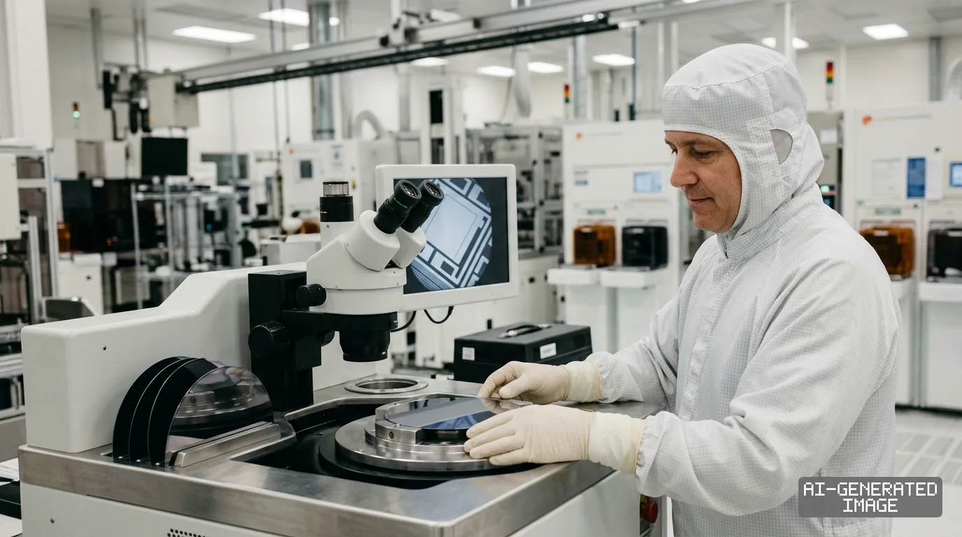
Samsung and SK hynix deploy cooling packaging on HBM4E chips
Both memory makers are re-engineering package thermal paths and copper bonding to contain heat dissipation bottlenecks on expanding silicon interposers.
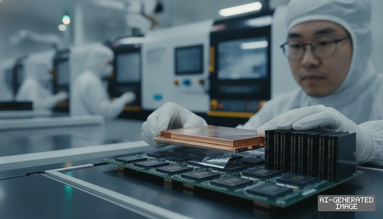
Samsung Electronics and SK hynix accelerated thermal packaging deployments on Oct. 12, 2026, targeting heat dissipation limits as AI interposers expand to support 16-layer HBM4E memory stacks.
Larger silicon interposers house multiple accelerator processors alongside high-bandwidth memory stacks. This dense integration concentrates thermal loads and causes structural warpage across the underlying substrate.
SK hynix embeds silicon cooling blocks to cut thermal resistance by 30%, the company said. Samsung Electronics uses power network tuning to lower thermal resistance by 10% on initial high-bandwidth stacks.
Both South Korean manufacturers are redesigning internal die interfaces. The shift reflects physical constraints as accelerator vendors prepare platforms that require data throughput exceeding four terabytes per second.
SK hynix unveiled its integrated cooling architecture, termed iHBM, on May 26, 2026. The architecture inserts non-conductive silicon structures directly into the base layers of the memory stack.
The company places these integrated cooling elements within the die-to-die physical layer. That interface connects the memory stack directly to the host accelerator and generates the highest heat density.
Direct heat channels pull thermal energy outward into external heat sinks. Conventional packages forced heat to travel through upper core memory dies before reaching the surface, SK hynix said.
SK hynix manufactures these packages with advanced mass reflow molded underfill technology. The technique injects liquid protective material between stacked dies to ensure structural stability without altering customer system layouts.
The supplier shipped 12-layer HBM4E samples operating at speeds up to 16 gigabits per second in June 2026. SK hynix plans to introduce the cooling element design across seventh-generation and eighth-generation lines.
Samsung Electronics approaches the thermal bottleneck through low-power circuitry and direct copper interfaces. The company commercialized its sixth-generation HBM4 memory on Feb. 12, 2026, using four-nanometer logic base dies.
Samsung redesigned its internal power distribution network to curb parasitic electrical resistance. That architecture improved heat dissipation by 30% compared to previous-generation HBM3E products, the company said.
Samsung displayed its seventh-generation HBM4E memory at the Nvidia GTC conference on March 17, 2026. The component achieved 16 gigabits per second per pin and 4.0 terabytes per second of bandwidth.
The manufacturer also presented hybrid copper bonding to assemble stacks reaching 16 layers or more. The process bonds copper pads directly between dies without using intermediary micro-bumps.
Eliminating micro-bumps reduces package height and tightens vertical thermal conduction paths. Samsung said the technique reduces thermal resistance by more than 20% compared to traditional thermal compression bonding.
The company completed initial shipments of 12-layer HBM4E samples on May 28, 2026. The design improved thermal resistance characteristics by 14% over baseline sixth-generation silicon, Samsung said.
Thermal dissipation has become the primary operational barrier for advanced accelerators. Expanding interposer surface areas increases thermal expansion mismatches between silicon dies, organic substrates and bonding layers.
When thermal expansion rates diverge under heavy data center workloads, interposers flex unevenly. That mechanical strain cracks micro-bump joints and degrades electrical continuity across memory channels.
Nvidia plans to integrate these dense memory stacks into its Vera Rubin computing platform. The architecture couples high-bandwidth memory with central processors and graphical processing units on single packaging substrates.
Memory suppliers must resolve mechanical warping before cloud service providers deploy these accelerator systems. Thermal degradation reduces overall computational throughput by forcing processors to throttle operating frequencies.
SK hynix relies on its established liquid underfill ecosystem to maintain assembly yields. Samsung relies on its integrated device manufacturing structure, combining in-house foundry fabrication with advanced packaging lines.
Both manufacturers expect qualification testing for 16-layer stacks to finish before volume production begins in early 2027. Customer validation milestones scheduled for November 2026 will determine production ramp allocations.
The companies did not disclose the commercial yield rates of their hybrid copper bonding lines. Neither manufacturer has published volume contract pricing for finished 16-layer HBM4E stacks.
Samsung continues engineering evaluations for custom memory logic dies at its Hwaseong packaging facility. SK hynix runs parallel thermal stress assessments with customer engineering teams in Icheon, South Korea.
Impact map
How this development propagates across the region and out to global buyers.
| Event | Korea | China | Japan | Global impact |
|---|---|---|---|---|
| HBM4E thermal packaging race | Samsung and SK hynix commercialize copper bonding and silicon cooling elements | Domestic memory makers remain constrained by micro-bump thermal dissipation limits | Packaging materials suppliers adapt liquid molding compounds for dense interposers | Hyperscale data center operators face higher packaging premiums on 16-layer AI chips |
In this story
- Companies
- Samsung ElectronicsSK hynix
- Tickers
- 005930.KS000660.KS
- Exposed
- Nvidia
- Policy
- Economic Security
- Impact
- Supply ChainCapexCost Structure
Track every Economic Security development →
Related briefings
- SK hynix and Samsung push 16-layer HBM4 as Nvidia caps Rubin at 12 dies Also on Nvidia, SK hynix, Samsung Electronics
- Samsung revamps HBM thermal packaging to challenge TSMC supply lead Also on Nvidia, SK hynix, Samsung Electronics
- SK hynix taps TSMC for 3D DRAM logic, diverging from Samsung in 2026 Also on Nvidia, SK hynix, Samsung Electronics
- TSMC widens CoWoS supply chain with $2 billion US interposer deal Also on Nvidia, SK hynix, Samsung Electronics
Sources
Reporting
Confidence: medium — how we grade this
The documents behind this briefing are linked above. East Asia Brief produces its English text with AI assistance under human editorial review, and does not translate or republish other outlets' articles. See our methodology and AI policy. Spotted an error? Tell us.
The Morning Brief
What changed in Korean, Chinese and Japanese industry overnight — and what it means for your supply chain. One email, weekday mornings, US time. Free.
The Morning Brief is in preparation. Leave your address and we will write to you once — when the first issue is ready. Nothing before that.