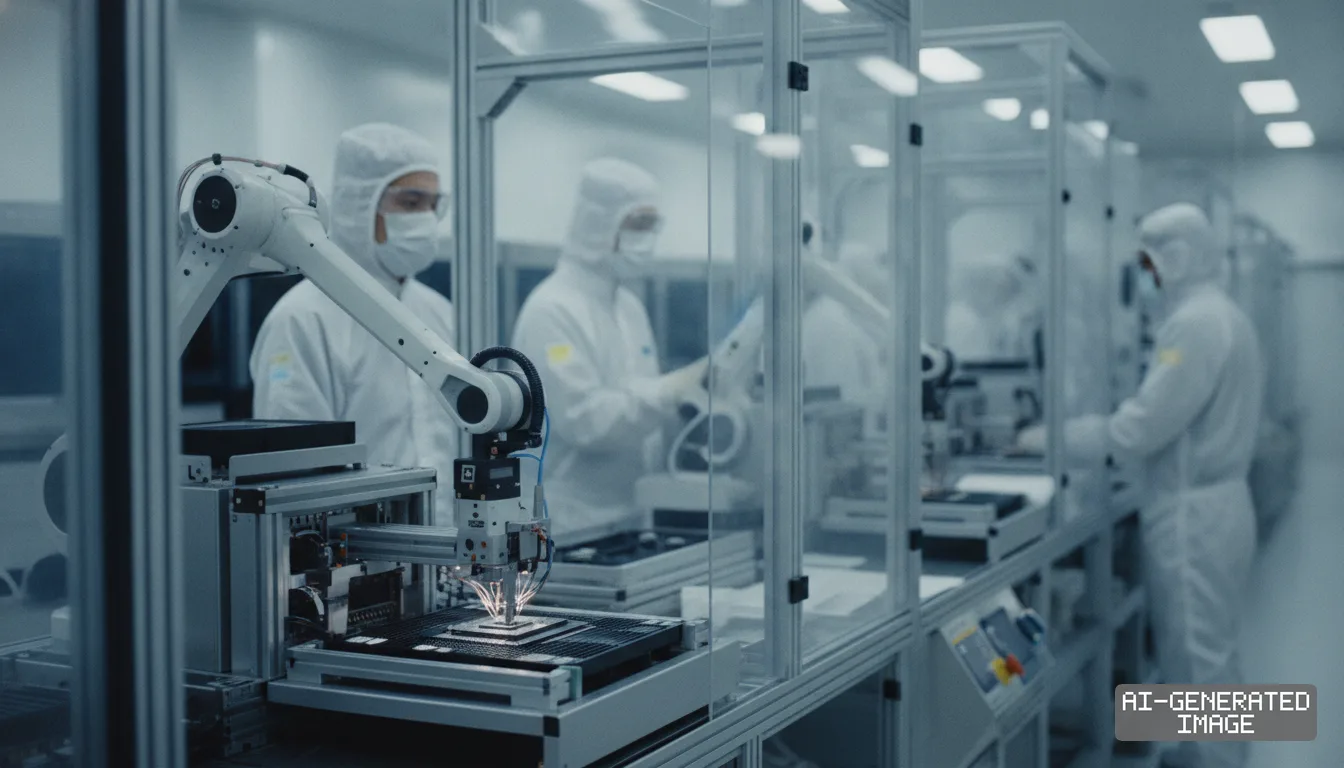
EO Technics takes 20% of laser wafer dicing from Japan's Disco
Shipments target thin-wafer packaging lines below 50 micrometers as high-bandwidth memory makers replace mechanical blades to curb silicon chipping.
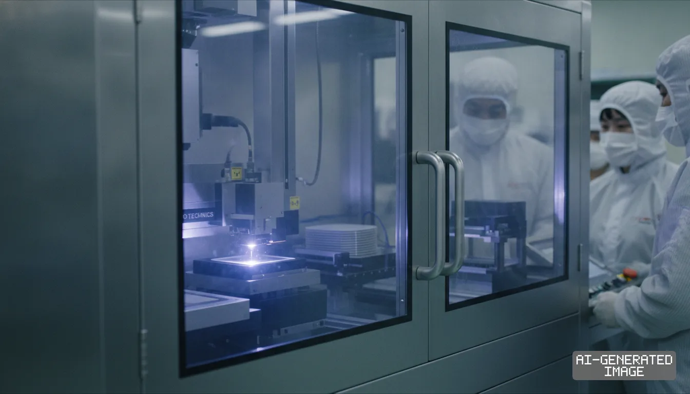
EO Technics expanded shipments of advanced laser grooving and dicing systems Nov. 12 to supply memory manufacturers accelerating next-generation packaging lines for artificial intelligence processors.
The equipment targets a 600 billion won ($440 million) global wafer dicing market previously dominated by Japan's Disco Corporation. Industry data show EO Technics securing between 15% and 20% of laser-based cutting installations.
Memory makers require silicon wafers thinned below 50 micrometers to build stacked high-bandwidth memory modules. Mechanical diamond blades cause micro-cracks and silicon edge chipping on wafers thinned to those specifications.
Mechanical stress during traditional saw cutting can also cause delamination — the peeling apart of microscopic wiring layers. Laser singulation eliminates direct physical contact, protecting fragile circuit paths along wafer cut lines.
Laser grooving systems prepare the wafer surface before final die separation takes place. The laser carves narrow trenches through low-k dielectric insulating films and copper metal layers deposited along the saw lanes.
Clearing those surface materials prevents diamond saws from gumming or tearing through brittle insulating layers. That trenching step improves final assembly yields on dense multi-layer semiconductor wafers.
EO Technics supplies the LMC3200G system for wafer grooving and the LMC3200D unit for wafer dicing, according to company catalog specifications. The dicing tool handles wafers thinned below 200 micrometers.
The non-contact dicing platform lowers operating costs because operators do not need to replace mechanical diamond blades. The company engineered the core laser components with semi-permanent service lifetimes to minimize maintenance downtime.
EO Technics previously delivered more than 10 femtosecond laser grooving units to outsourced semiconductor assembly and test providers. The deliveries supplied Taiwan's ASE Technology Holding, US-based Amkor Technology and China's JCET Group.
Those packaging contractors installed the femtosecond systems to process next-generation artificial intelligence chips and mobile processors. The deployments demonstrated that the company's laser sources met commercial volume manufacturing standards overseas.
South Korean memory producers then began qualifying the domestic laser tools for high-bandwidth memory lines. Samsung Electronics installed laser grooving tools at its Cheonan packaging facility and deployed stealth dicing units in Pyeongtaek.
Stealth dicing focuses an internal laser beam inside the silicon substrate rather than ablating the wafer surface. A subsequent tape-expansion process separates individual dies cleanly along the internally modified thermal fracture lines.
Micron Technology also integrated laser wafer cutting systems into its memory packaging operations in Taiwan. SK hynix initiated production-line evaluations to qualify alternative domestic laser equipment for its advanced memory packaging operations.
The supplier diversification challenges Disco Corporation, which maintains an installed base exceeding 60% of the worldwide wafer saw market. Disco historically protected its market share by bundling grooving tools with mechanical dicers.
EO Technics designed its grooving systems to interface directly with existing Disco blade dicers, according to research by Kyobo Securities. That compatibility allows semiconductor manufacturers to adopt alternative grooving tools without replacing entire dicing bays.
Packaging lines are accelerating laser adoption as memory architectures shift from eight-layer stacks toward 12-layer and 16-layer configurations. Thinner dies must be placed closer together to keep overall module heights within industry standards.
Laser cutting enables chipmakers to narrow wafer street widths between dies by several micrometers. Narrower streets permit foundries to fit additional functional dies onto each 300-millimeter silicon wafer, reducing cost per die.
Upcoming HBM4 products will incorporate custom logic base dies fabricated on advanced foundry nodes below five nanometers. The fine metallization patterns on those logic wafers require precision laser cutting rather than mechanical shearing.
Shares of EO Technics closed down 1.47% at 362,500 won on the KOSDAQ market Nov. 12. The company rarely conducts public investor relations conferences or voluntary regulatory filings regarding order intake.
EO Technics has not published a regulatory filing confirming specific contract values, customer names or delivery timelines tied to the Nov. 12 equipment shipments.
Memory producers will finalize vendor qualification rosters for commercial HBM4 assembly lines by the first quarter of 2027. EO Technics must file its audited full-year financial statements with the Korea Exchange by March 31, 2027.
Impact map
How this development propagates across the region and out to global buyers.
| Event | Korea | China | Japan | Global impact |
|---|---|---|---|---|
| Laser dicing tool adoption | Samsung Electronics and SK hynix qualify domestic grooving tools to lower die damage | JCET Group installs femtosecond grooving systems to package logic dies | Disco Corporation defends a 60% mechanical saw share as laser grooving erodes bundles | OSATs narrow wafer saw lanes to lift chip yields from 300-millimeter wafers |
In this story
- Companies
- EO TechnicsDisco Corporation
- Tickers
- 039030.KQ6146.T
- Exposed
- Samsung ElectronicsSK hynixMicron TechnologyASE Technology HoldingAmkor TechnologyJCET Group
- Impact
- Supply ChainOrder BookCost Structure
Related briefings
- South Korean toolmakers advance glass substrate TGV laser drillers to volume lines Also on EO Technics, Order Book
- Silicon interposer scaling drives foundry and OSAT shifts in 3.5D chiplets Also on JCET Group, ASE Technology Holding, Amkor Technology
- JCET expands automotive radar SiP packaging lines to capture ADAS sensor demand Also on JCET Group, ASE Technology Holding, Amkor Technology
- East Asian SiC wafer makers shift to laser slicing to cut 8-inch ingot processing loss Also on DISCO Corporation, Cost Structure
Sources
Primary documents
Reporting
Confidence: high — how we grade this
The documents behind this briefing are linked above. East Asia Brief produces its English text with AI assistance under human editorial review, and does not translate or republish other outlets' articles. See our methodology and AI policy. Spotted an error? Tell us.
The Morning Brief
What changed in Korean, Chinese and Japanese industry overnight — and what it means for your supply chain. One email, weekday mornings, US time. Free.
The Morning Brief is in preparation. Leave your address and we will write to you once — when the first issue is ready. Nothing before that.