TSMC taps affiliate Xintec for CoWoS packaging through 2033
The foundry giant supplies Taichung cleanroom space while Xintec issues NT$15 billion in convertible bonds to install dedicated advanced backend tooling.
Taiwan Semiconductor Manufacturing Company signed a seven-year packaging agreement with affiliate Xintec on Nov. 13, 2026, outsourcing backend assembly to ease capacity shortages for artificial intelligence accelerators.
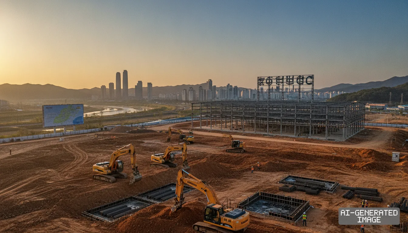
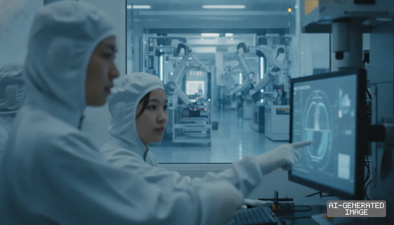
The agreement runs from Nov. 13, 2026 through Dec. 31, 2033. Under the contract, TSMC will provide cleanroom space inside its facilities at the Central Taiwan Science Park in Taichung, while Xintec installs and runs dedicated production lines.
Xintec approved a NT$15 billion ($456 million) convertible bond issuance on Nov. 13 to finance the initial capital expenditure. The proceeds will fund production equipment and automated material handling systems, which transport wafer carriers across manufacturing bays.
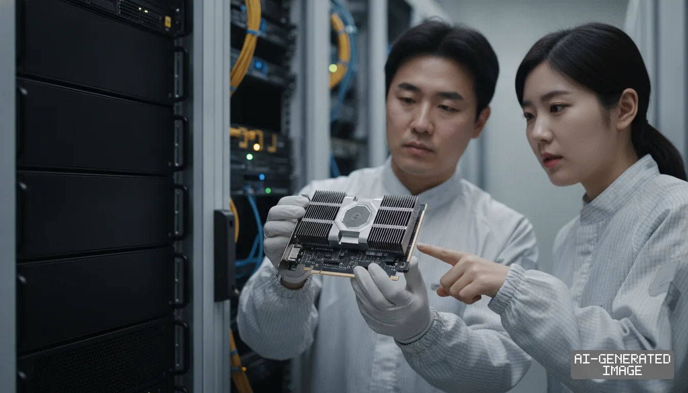
The outsourced work focuses specifically on the on-substrate stage of chip-on-wafer-on-substrate packaging. The architecture integrates graphic processors and high-bandwidth memory chips on a single silicon platform to accelerate data transfer.
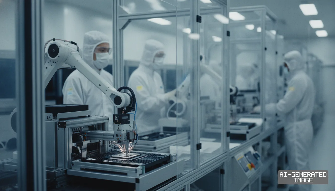
Chip-on-wafer-on-substrate packaging consists of two primary operational steps. The first step attaches processed silicon dies onto an intermediate silicon interposer. The second step mounts that combined module onto a multi-layer ball grid array substrate.
TSMC is keeping the front-end die stacking inside its proprietary fabs. Xintec will handle the downstream on-substrate assembly, where completed modules are bonded to circuit boards and sealed for system assembly.
Separating the packaging steps allows TSMC to free cleanroom capacity for lithography and high-density interposer bonding. The split transfers lower-margin, floor-space-intensive substrate assembly to an external partner without relinquishing operational control.
TSMC owns an equity stake of about 41% in Xintec. The packaging house depends on TSMC contract manufacturing for more than 70% of its annual operating revenue.
The corporate tie gives TSMC direct visibility into yield rates and tool utilization. The arrangement functions as an internal joint venture located on TSMC property rather than an arm's-length supply agreement.
Capacity constraints in advanced packaging remain the primary bottleneck restricting shipments of artificial intelligence processors. Leading accelerator designers such as Nvidia have booked large shares of advanced packaging availability through 2027.
Customers building large language models require clusters of processors wired directly to high-bandwidth memory stacks. Conventional assembly techniques cannot provide the microscopic wiring density required to prevent transmission delays between logic and memory dies.
Demand has outpaced available cleanroom footprint across western Taiwan. TSMC has been reallocating existing plant space and purchasing older flat-panel display fabs to convert into packaging lines.
The Xintec partnership mirrors earlier packaging outsourcing programs with outsourced semiconductor assembly and test providers. Companies such as ASE Technology Holding and Amkor Technology have long packaged modules using licenses provided by TSMC.
Those external OSAT vendors run on-substrate lines in their own facilities. By contrast, the Xintec contract embeds the contractor inside TSMC's Taichung fab complex to minimize transit damage and logistics turnaround.
The Taichung site integrates automated overhead hoist transport tracks connecting fab modules. Installing Xintec lines inside the same perimeter eliminates regional road freight between front-end interposer production and backend substrate mounting.
Xintec plans to begin commercial mass production on the new lines in 2029. The multi-year lead time reflects the procurement schedules for specialized thermocompression bonders, underfill dispensers and automated optical inspection equipment.
Capital equipment suppliers must customize tooling to match TSMC's automated defect-tracking protocols. Xintec said engineering teams will collaborate directly with TSMC personnel to guarantee that production lines achieve identical yield benchmarks.
The seven-year framework assures Xintec of stable volume allocation across economic cycles. Long-term off-take commitments protect contract packagers from carrying idle depreciation costs if merchant chip orders fluctuate.
For enterprise customers, the contract establishes an expanded packaging pipeline heading into the next decade. High-performance computing developers have sought multi-year capacity guarantees before committing capital to next-generation silicon tape-outs.
The regulatory filing does not state the targeted monthly wafer processing capacity for the 2029 installation, and TSMC has not issued a stand-alone release on the transaction.
Under the timetable established on Nov. 13, Xintec will proceed with issuing the NT$15 billion in convertible bonds while preparing cleanroom installations ahead of the 2029 manufacturing debut. The operating agreement remains binding through Dec. 31, 2033.
Impact map
How this development propagates across the region and out to global buyers.
| Event | Korea | China | Japan | Global impact |
|---|---|---|---|---|
| CoWoS packaging outsourcing | Memory suppliers gain stable downstream demand for high-bandwidth memory stacks | Domestic packaging firms face wider technological gap in 2.5D accelerator assembly | Equipment vendors take orders for automated handling and inspection tools | AI chip designers secure expanded advanced packaging supply through 2033 |
| CoWoS packaging outsourcing | Memory suppliers gain stable downstream demand for high-bandwidth memory stacks | Domestic packaging firms face wider technological gap in 2.5D accelerator assembly | Equipment vendors take orders for automated handling and inspection tools | AI chip designers secure expanded advanced packaging supply through 2033 |
In this story
- Companies
- TSMCXintec
- Tickers
- 2330.TW3374.TWO
- Exposed
- NvidiaASE Technology HoldingAmkor Technology
- Impact
- Supply ChainCapexCapacity
Related briefings
- TSMC Buys AUO Fabs for $1.2B to Expand Advanced Packaging Also on Xintec, TSMC, Nvidia
- TOPPAN and Broadcom open Singapore plant for AI substrates Also on Capacity
- Foundry 2.0 Revenue Climbs 25% Also on ASE Technology Holding, Amkor Technology, TSMC
- Intel pits EMIB-T packaging against TSMC to win AI chip orders Also on ASE Technology Holding, Amkor Technology, Nvidia
Sources
Primary documents
Reporting
Confidence: high — how we grade this
The documents behind this briefing are linked above. East Asia Brief produces its English text with AI assistance under human editorial review, and does not translate or republish other outlets' articles. See our methodology and AI policy. Spotted an error? Tell us.
The Morning Brief
What changed in Korean, Chinese and Japanese industry overnight — and what it means for your supply chain. One email, weekday mornings, US time. Free.
The Morning Brief is in preparation. Leave your address and we will write to you once — when the first issue is ready. Nothing before that.