East Asian SiC wafer makers shift to laser slicing to cut 8-inch ingot processing loss
Slicing and polishing yield disparities across Japan, China and South Korea redefine 200-millimeter silicon carbide substrate economics for automotive device makers.
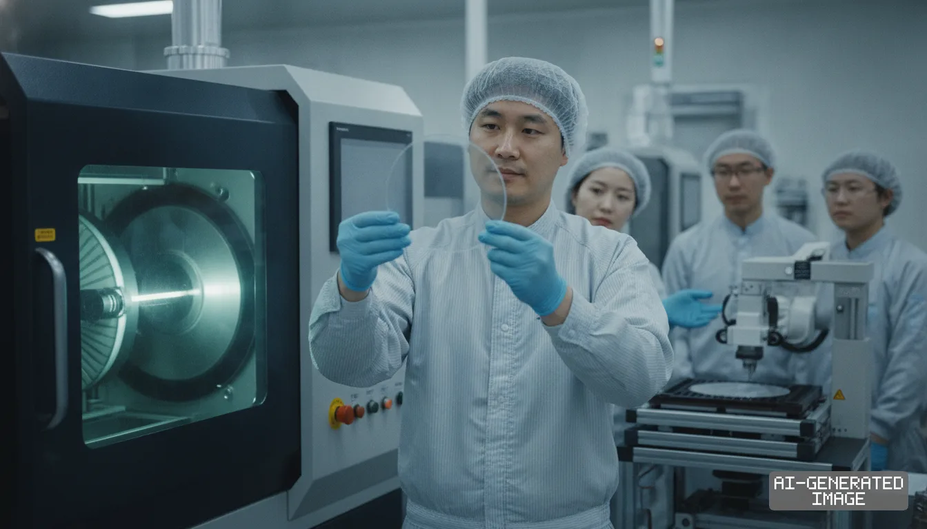
East Asian power semiconductor manufacturers are shifting from multi-wire sawing to laser slicing and advanced abrasive polishing to eliminate severe material losses and reduce production bottlenecks in 200-millimeter (8-inch) silicon carbide (SiC) wafer manufacturing.
The transition to 200-millimeter substrates represents the primary technical lever for power device makers seeking to lower the manufacturing cost of SiC MOSFETs used in 800-volt electric vehicle traction inverters. Silicon carbide ranks among the hardest known materials, making the mechanical conversion of single-crystal ingots into pristine semiconductor-grade substrates exceptionally slow and resource-intensive. Conventional diamond multi-wire sawing consumes roughly 50 percent of the raw crystal boule as kerf loss the material turned into useless dust during cutting. Subsequent grinding, lapping, and chemical mechanical polishing (CMP) stages inflict further material degradation, dragging cumulative effective substrate yields down to approximately 75 percent due to the removal of roughly 250 micrometers of crystal per finished wafer.
The documents behind this briefing are linked above. East Asia Brief produces its English text with AI assistance under human editorial review, and does not translate or republish other outlets' articles. See our methodology and AI policy. Spotted an error? Tell us.