TSMC and Samsung embed liquid microchannels into AI packages
Foundries and memory producers are running coolant directly over active silicon as accelerator package power requirements surge from 600 watts to 4,100 watts by 2029.
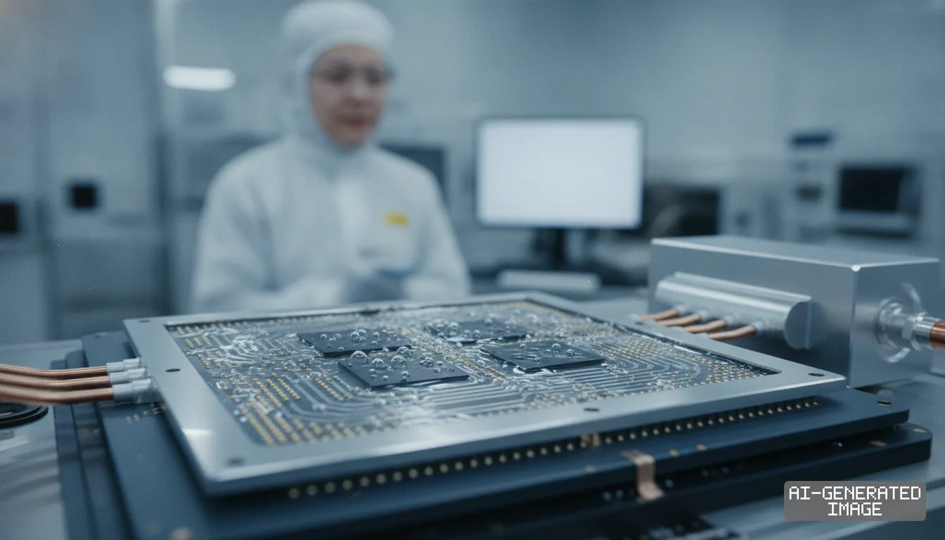
Taiwan Semiconductor Manufacturing Co., Samsung Electronics and SK hynix accelerated efforts on Nov. 11, 2026, to integrate microchannel liquid cooling directly into silicon packages to cool next-generation artificial intelligence accelerators.
The shift addresses a thermal threshold where external copper cold plates can no longer extract heat fast enough. Moving liquid directly over active silicon eliminates the thermal barrier created by conventional interface materials.
Package power will expand from 600 watts in 2024 to 4,100 watts by 2029. That 583% increase will accompany a 48-fold expansion in compute transistors and a 34-fold jump in memory bandwidth within single packages.
TSMC added microchannel cooling to its official advanced packaging roadmap to handle multi-kilowatt packages. The foundry has demonstrated lab test vehicles dissipating over 5 kilowatts using Chip-on-Wafer-on-Substrate with redistribution layers.
Thermal interface materials—greases and solders placed between chips and external plates—account for a large share of package thermal resistance. Etching microscopic conduits into package lids and silicon dies eliminates that resistance layer.
James Chen, director of advanced packaging development at TSMC, presented the 4,100-watt projection at SEMICON Taiwan. Power delivery losses will rise more than fivefold as package areas expand past 14 reticle sizes, Chen said.
By 2028, TSMC plans to produce packaging structures housing roughly 10 compute dies and 20 high-bandwidth memory stacks. Managing heat across that surface requires circulating fluid within fractions of a millimeter from active circuits.
Samsung Electronics registered a patent with the U.S. Patent and Trademark Office on Oct. 20, 2026, for an internal chip-cooling architecture. The design etches micro-conduits inside the silicon body.
The patent incorporates a suspended wick structure that uses capillary action to circulate liquid without external high-pressure pumps. The mechanism absorbs thermal spikes at localized hot spots and draws vapor toward integrated condensing regions.
Samsung plans to apply the internal conduit structure across its foundry and memory lines. The approach targets high-density computing modules where vertical die stacks trap thermal loads inside lower layers.
SK hynix unveiled its iHBM technology on May 26, 2026, to tackle heat at memory interfaces. The company embeds Integrated Cooling Elements directly into the memory package stack.
These cooling elements consist of electrically non-conductive, thermally conductive silicon blocks. SK hynix positions them directly over the physical interconnect layer connecting the memory base die to host processors.
The design lowers thermal resistance by more than 30% compared with conventional packages, SK hynix said. The company applies its mass-reflow molded underfill process to produce the cooling-integrated memory modules at commercial scale.
Thermal concentration is acute at the interconnect boundary where thousands of micro-bumps transmit high-frequency data. Traditional architectures vent heat upward through DRAM layers, degrading retention times in the upper silicon cells.
Academic researchers have also proved that micro-channel architectures can handle heat fluxes far beyond commercial limits. A team at the Korea Advanced Institute of Science and Technology published fluid validation data on June 15, 2026.
The research team removed heat fluxes exceeding 2,000 watts per square centimeter using manifold microchannels etched in silicon. The test ran under a low pumping pressure of 8 kilopascals, achieving a coefficient of performance above 100,000.
Circulating water through sub-millimeter channels inside silicon reduces the pumping power needed in hyperscale data centers. The manifold design divides fluid flow into short paths, preventing pressure drops and hot-spot saturation across the die.
Direct silicon cooling forces sweeping changes down the packaging supply chain. Substrate makers must redesign core panels to prevent warpage when liquid channels create asymmetric thermal expansion across the package.
Epoxy molding compound suppliers must formulate materials that resist chemical degradation from prolonged contact with dielectric fluids and deionized water. Moisture absorption within packaging resins risks electrical shorts and delamination under continuous 85°C server operation.
Hyperscalers are accelerating trials of embedded liquid packaging to fit rack-level limits. Nvidia set a 100% liquid-cooled specification for its incoming rack architectures using 45°C warm-water loops to eliminate power-hungry chillers.
Standardizing internal fluid connections remains a hurdle for contract manufacturers. Fluid quick-disconnect couplings must shrink to package dimensions while guaranteeing zero leaks over five-year server lifespans.
Commercial qualification of direct-die liquid channels faces reliability testing in 2027, ahead of TSMC's planned 14-reticle package ramp in 2028. Foundries are conducting thermal cycling tests to evaluate microchannel erosion under continuous flow.
Chipmakers have not published standardized fluid interface specifications or production yield loss figures for direct-etched silicon microchannels. Foundries have also not disclosed whether micro-channel manufacturing will require dedicated etch equipment in back-end assembly facilities.
Supply contracts for advanced packaging will increasingly hinge on integrated thermal architectures rather than transistor density alone. Foundry customers will audit fluid reliability data alongside silicon defects as accelerator power passes 1,000 watts per die.
Impact map
How this development propagates across the region and out to global buyers.
| Event | Korea | China | Japan | Global impact |
|---|---|---|---|---|
| In-package microchannel cooling transition | Samsung patents capillary conduits; SK hynix embeds ICE to lower memory thermal resistance 30% | Packaging assemblers face retrofit capex for specialized fluid sealing lines | Chemical suppliers reformulate epoxy molding compounds and underfills for liquid resistance | AI server clusters eliminate chillers using 45°C warm-water loops to cool 4,100W packages |
In this story
- Companies
- Taiwan Semiconductor Manufacturing Co.Samsung ElectronicsSK hynix
- Tickers
- 2330.TW005930.KS000660.KS
- Exposed
- Nvidia
- Impact
- Supply ChainCapexCost Structure
Related briefings
- SK hynix speeds HBM4 design with Nvidia physics simulation tools Also on Taiwan Semiconductor Manufacturing Co., Nvidia, SK hynix
- Intel pits EMIB-T packaging against TSMC to win AI chip orders Also on Taiwan Semiconductor Manufacturing Co., Nvidia, SK hynix
- GlobalFoundries signs $2 billion TSMC chip interposer deal Also on Taiwan Semiconductor Manufacturing Co., Nvidia, SK hynix
- TSMC and Samsung unify 3nm base die specs for Nvidia custom HBM Also on Taiwan Semiconductor Manufacturing Co., Nvidia, SK hynix
Sources
Reporting
Confidence: medium — how we grade this
The documents behind this briefing are linked above. East Asia Brief produces its English text with AI assistance under human editorial review, and does not translate or republish other outlets' articles. See our methodology and AI policy. Spotted an error? Tell us.
The Morning Brief
What changed in Korean, Chinese and Japanese industry overnight — and what it means for your supply chain. One email, weekday mornings, US time. Free.
The Morning Brief is in preparation. Leave your address and we will write to you once — when the first issue is ready. Nothing before that.