SK hynix taps TSMC for 3D DRAM logic, diverging from Samsung in 2026
The memory maker is outsourcing peripheral circuit fabrication to Taiwanese foundries, challenging Samsung Electronics' vertical integration model as DRAM scaling reaches physical limits.
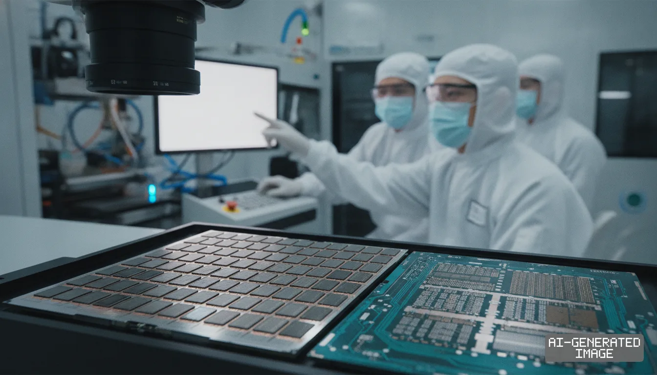
SK hynix on Sept. 14 accelerated its technical shift toward external foundries for 3D DRAM peripheral logic, reinforcing an open-architecture manufacturing alliance with Taiwan Semiconductor Manufacturing Co.
Peripheral circuitry accounts for roughly 30% of a conventional DRAM chip footprint. The architectural transition frees silicon area by relocating routing circuits underneath vertically stacked memory cell arrays.
SK hynix has not published dedicated capital spending figures for its 3D DRAM pilot lines. DRAM products generated 68% of the company's 16.42 trillion won ($12.1 billion) revenue in the second quarter.
The strategy formalizes technical directions disclosed at the 2026 SK hynix Future Forum held on Sept. 8 in Icheon. Company executives identified peripheral foundry integration as essential to overcome physical limits in monolithic scaling.
Vice presidents Kim Kyeong-hoon, Kim Hyung-soo and Son Ho-young outlined three core development priorities. The engineers committed to maximizing data bus bandwidth, adopting ultra-short reach interconnects and tapping pure-play foundries for control circuits.
April Lee, director of AI and high-performance computing business development at TSMC, attended the Icheon forum as a panelist. The technical session examined memory-logic convergence required for next-generation artificial intelligence accelerators.
Conventional planar DRAM faces severe electrical leakage and capacitor thinning below the 10-nanometer barrier. Stacking memory cells vertically into three dimensions allows chipmakers to increase bit density without shrinking horizontal transistor gates.
Standard memory wafer fabs use thermal processes that degrade high-performance logic transistors. Transferring peripheral circuitry to an advanced pure-play foundry allows SK hynix to build control logic on smaller, faster lithography nodes.
SK hynix presented the underlying framework at the TSMC Technology Symposium on April 23 in California. The company confirmed joint development roadmaps covering 3D-stacked DRAM-on-logic structures and high-bandwidth flash memory.
The arrangement expands an established partnership between the two Asian chipmakers. SK hynix already relies on TSMC advanced logic nodes to fabricate the base die for 16-layer HBM4 modules.
Samsung Electronics has taken a contrasting approach by keeping all 3D memory manufacturing inside its corporate perimeter. The Suwon-based company operates an integrated device manufacturer model that combines design, foundry and assembly.
Samsung is developing four-square-femto-meter vertical-channel transistors entirely through its internal fabrication network. The company assigns peripheral base die production to its proprietary SF4 four-nanometer foundry lines rather than contracting third-party fabs.
Samsung also handles advanced packaging in-house through its Saint and I-Cube production lines. The closed system prevents external fabricators from reviewing proprietary cell architectures, interface registries and internal timing parameters.
Samsung commands roughly 41% of the global DRAM market across data center servers and mobile devices. Its integrated model captures full manufacturing margins without paying outside wafer fabrication or packaging fees.
SK hynix controls approximately 34% of worldwide DRAM supply and over 50% of the high-bandwidth memory sector. TSMC produces more than 60% of global contract logic wafers, giving it unequaled manufacturing scale.
The alliance strategy exposes SK hynix to external wafer pricing cycles and foundry allocation schedules in Taiwan. The company must also synchronize product development calendars across separate corporate engineering organizations.
Partnering with TSMC grants SK hynix immediate access to sub-three-nanometer logic nodes without building proprietary logic fabs. Advanced logic fabs require capital expenditures exceeding $15 billion per facility, according to industry estimates.
The approach also aligns SK hynix with Nvidia and other major accelerator designers that manufacture primary compute tiles at TSMC. Direct packaging compatibility streamlines final assembly for high-performance AI clusters.
SK hynix has not published a binding joint development contract or exclusive supply agreement with TSMC for dedicated 3D DRAM manufacturing. Neither company has disclosed commercial revenue splits or proprietary royalty structures.
SK hynix plans to complete qualification tape-outs for TSMC-fabricated HBM4 base dies in the fourth quarter of 2025. Engineering evaluation runs for monolithic 3D DRAM architectures are scheduled for customer testing in late 2027.
Commercial mass production of 3D DRAM across the semiconductor industry is targeted for 2028. Pilot lines at SK hynix facilities in Icheon and Samsung fabs in Hwaseong continue running test wafers.
Impact map
How this development propagates across the region and out to global buyers.
| Event | Korea | China | Japan | Global impact |
|---|---|---|---|---|
| 3D DRAM architecture divergence | SK hynix cuts logic capex while Samsung internalizes SF4 base dies | CXMT faces wider architectural gap in sub-10nm memory transitions | Tokyo Electron and Canon supply hybrid bonding tools to both camps | AI chip designers gain multi-source base die options for next-gen accelerators |
In this story
- Companies
- SK hynixTSMCSamsung Electronics
- Tickers
- 000660.KS2330.TW005930.KS
- Exposed
- Nvidia
- Policy
- Economic Security
- Impact
- Supply ChainCapexCost Structure
Track every Economic Security development →
Related briefings
- TSMC Urges HBM Makers to Adopt X-Ray Friendly Chip Design for Advanced Packaging Also on TSMC, Nvidia, SK hynix
- East Asia materials makers accelerate diamond heat spreaders for 1000W AI chips Also on TSMC, Nvidia, SK hynix
- Japanese epoxy mold makers reformulate resins to tame warpage in 16-high memory Also on TSMC, Nvidia, SK hynix
- OpenAI denies Samsung foundry deal for custom AI processors Also on TSMC, Nvidia, SK hynix
Sources
Reporting
Confidence: medium — how we grade this
The documents behind this briefing are linked above. East Asia Brief produces its English text with AI assistance under human editorial review, and does not translate or republish other outlets' articles. See our methodology and AI policy. Spotted an error? Tell us.
The Morning Brief
What changed in Korean, Chinese and Japanese industry overnight — and what it means for your supply chain. One email, weekday mornings, US time. Free.
The first issue goes out shortly. Sign up now and you will not miss it.