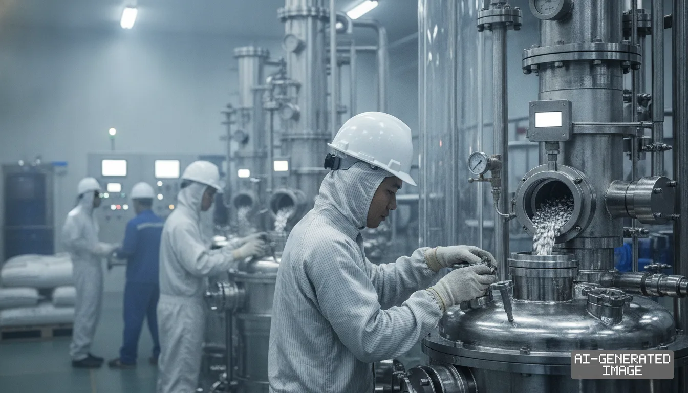
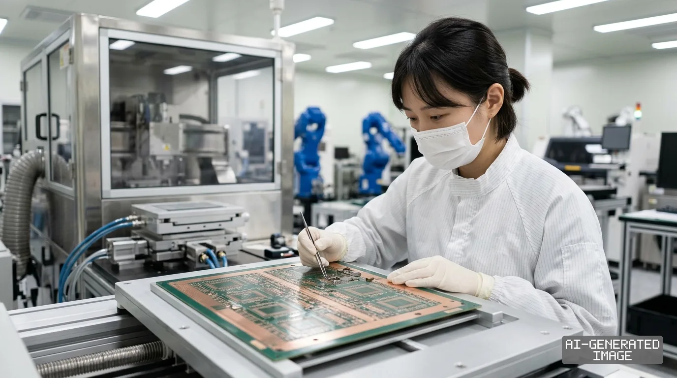
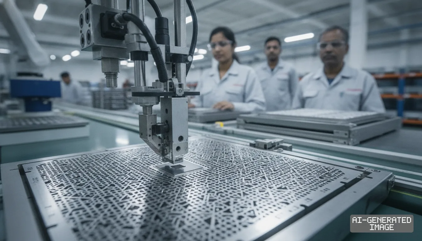
Samsung revamps HBM thermal packaging to challenge TSMC supply lead
The South Korean chipmaker pairs 4nm base dies with hybrid copper bonding to curb thermal resistance by 20% as Nvidia demands tighter packaging height limits.
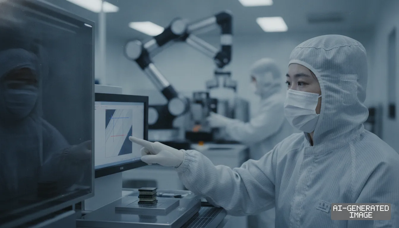
Samsung Electronics Co. encountered tighter thermal tolerances on Oct. 6, 2026, when Nvidia Corp. requested memory makers reduce high-bandwidth memory heights five micrometers below standard dimensions.
The change requires suppliers to trim total package height from the 775-micrometer ceiling set by the JEDEC Solid State Technology Association. The request tightens physical margins for next-generation AI processors.
Samsung builds high-bandwidth memory alongside contract foundry lines. This dual structure positions the company to compete directly against Taiwan Semiconductor Manufacturing Co., which dominates graphics processor packaging through its Chip-on-Wafer-on-Substrate line.
The Suwon-based company shipped commercial HBM4 modules built on its 1c-nanometer DRAM and a 4nm logic base die on Feb. 12. Those units cut thermal resistance by 10% and improved heat dissipation by 30% over HBM3E.
Samsung achieved those thermal reductions through low-voltage through-silicon vias and power distribution network tuning. The redesign also raised energy efficiency by 40% compared to previous memory stacks, the company said.
Packaging height limits grow more severe as customers stack 12 and 16 memory dies within standard server slots. Stacking thinner silicon chips increases mechanical warping during thermal assembly.
Nvidia commands more than 80% of data center graphics processors worldwide. That dominant market share allows the company to enforce sub-millimeter packaging requirements across memory partners.
TSMC expanded its dedicated CoWoS packaging capacity to meet those specifications. The Taiwanese foundry relies on external memory suppliers, assembling stacks produced by SK hynix Inc. and Micron Technology Inc.
Samsung offers an alternative model through internal turnkey packaging. The company fabricates logic base dies, manufactures dynamic memory, and completes advanced packaging inside its own facilities.
Thermal management forms the main physical barrier in this packaging competition. Heat from underlying logic dies transfers directly into stacked memory, raising operating temperatures across the graphics assembly.
To address heat buildup in taller stacks, Samsung presented hybrid copper bonding for HBM4E at Nvidia GTC on March 17. The method removes microbumps to join copper pads directly between silicon layers.
Hybrid copper bonding lowers thermal resistance by more than 20% compared to thermal compression bonding, Samsung said. The technique eliminates non-conductive film layers that retain heat between dies.
Samsung extended its commercial commitments on July 24 by signing an infrastructure agreement with Broadcom Inc.. The deal outlines $200 billion in memory, 2nm foundry and packaging work through 2030.
Broadcom designs custom application-specific accelerators for cloud computing hyperscalers. The partnership directs multi-die packaging orders directly into Samsung manufacturing lines rather than third-party packaging houses.
Competitors also face structural heat constraints in dense servers. SK hynix supplies the majority of HBM3E stacks for current Nvidia systems, relying on mass reflow molded underfill technology.
That assembly technique uses liquid epoxy to fill gaps between memory dies. As stacks reach 16 layers, epoxy layers resist thermal transfer more than direct copper connections.
Samsung plans to apply a heat path block design to eighth-generation HBM5 memories. The architectural concept routes heat away from central hot spots toward exterior dissipation plates.
The company integrated similar cooling structures into mobile application processors before adapting the architecture for high-density computing. Engineering teams are tailoring the heat blocks for two-nanometer base dies.
Customer delivery schedules dictate the pace of packaging adoption. Samsung scheduled initial customer qualification for 16-layer HBM4E components in early 2027 following sample shipments completed in May.
The commercial schedule depends on customer verification across multi-chip modules. AI hyperscalers test memory samples alongside proprietary compute dies before clearing volume production.
Samsung Electronics has not published a formal filing on Oct. 6, 2026 confirming an immediate overhaul of thermal interface materials specifically countering TSMC capacity additions.
Memory suppliers must confirm whether production lines can sustain high yields under the five-micrometer thickness reduction before volume shipments begin next quarter.
Impact map
How this development propagates across the region and out to global buyers.
| Event | Korea | China | Japan | Global impact |
|---|---|---|---|---|
| HBM packaging thermal tolerances | Samsung deploys turnkey packaging and hybrid copper bonding to offset a 5-micrometer package height reduction | Domestic AI accelerator builders face tighter packaging access under foundry restrictions | Material suppliers face higher purity standards for copper bonding and thermal interface films | AI server module yields face tighter physical margins under sub-775-micrometer height specifications |
In this story
- Companies
- Samsung Electronics
- Tickers
- 005930.KS
- Exposed
- NvidiaTSMCBroadcomSK hynix
- Policy
- Economic Security
- Impact
- Supply ChainCapexCost Structure
Track every Economic Security development →
Related briefings
- Samsung narrows SK hynix HBM lead as HBM4 shipments expand Also on Broadcom, TSMC, Nvidia
- TSMC sees 3nm revenue overtake 5nm node on surge in AI accelerators Also on Broadcom, Nvidia, Samsung Electronics
- Silicon interposer scaling drives foundry and OSAT shifts in 3.5D chiplets Also on Broadcom, Samsung Electronics, Cost Structure
- TOPPAN and Broadcom open Singapore plant for AI substrates Also on Broadcom
Sources
Reporting
Confidence: medium — how we grade this
The documents behind this briefing are linked above. East Asia Brief produces its English text with AI assistance under human editorial review, and does not translate or republish other outlets' articles. See our methodology and AI policy. Spotted an error? Tell us.
The Morning Brief
What changed in Korean, Chinese and Japanese industry overnight — and what it means for your supply chain. One email, weekday mornings, US time. Free.
The Morning Brief is in preparation. Leave your address and we will write to you once — when the first issue is ready. Nothing before that.