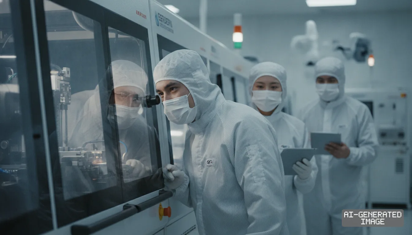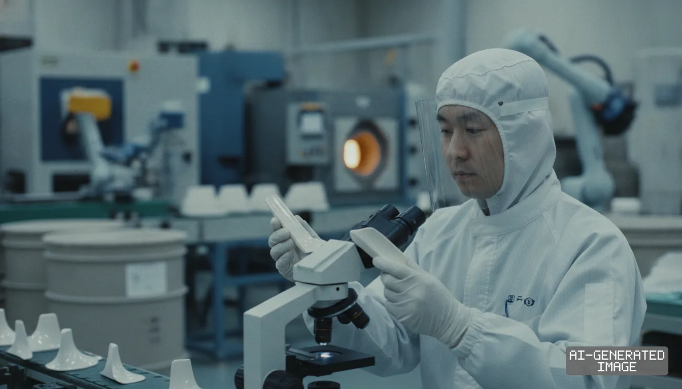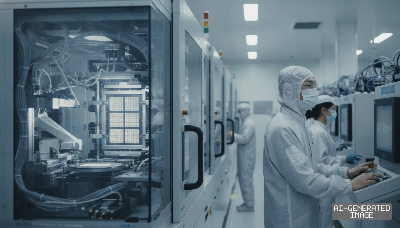
Samsung and SK hynix upgrade China memory fabs to 286 layers
The South Korean memory makers confirmed line retooling under U.S. consultations, moving Xi'an and Dalian sites past 200 layers as domestic rival YMTC captures market share.
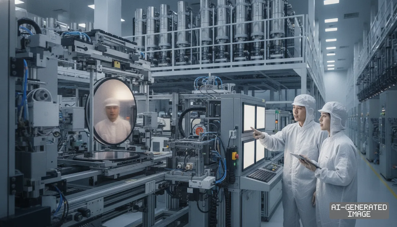
Samsung Electronics and SK hynix confirmed Oct. 21, 2026, they are upgrading their Chinese NAND flash memory manufacturing plants, pushing process nodes past 200 layers to protect market share against rising domestic competition.
Samsung is converting its Xi'an facility in northwestern China to make 286-layer ninth-generation V-NAND chips under an internal initiative called Monami. The Xi'an complex accounts for about 40% of Samsung's global NAND flash memory output.
The conversion targets initial output of 5,000 wafers a month in December 2026. Samsung plans to lift that volume to 40,000 wafers a month by December 2027, according to project plans reviewed by industry officials.
Samsung plans to run eighth-generation and ninth-generation lines in parallel at the Xi'an site throughout the transition. The dual-track schedule aims to sustain baseline chip shipments while cleanrooms install higher-density equipment.
SK hynix is preparing a parallel manufacturing shift at its NAND facility in Dalian, China. The company aims to move equipment currently running 192-layer manufacturing lines to fabricate memory devices stacked to 240 layers and above.
Both memory makers said the upgrades are proceeding in close consultation with the U.S. government. Neither firm disclosed operational wafer targets or equipment spending totals in their official written responses.
The technological upgrades come as Chinese state-backed memory producer Yangtze Memory Technologies Co., or YMTC, erodes South Korean dominance. YMTC captured 38.5% of China's NAND market in the second quarter of 2026.
Samsung fell to second place with a 33.5% share in China during the second quarter, market tracking data from Omdia showed. SK hynix held third place with a 17% share across Chinese commercial channels.
Surging demand for enterprise solid-state storage from artificial intelligence data centers has driven the retooling push. Without newer process nodes, Chinese fabs risk sliding into low-margin legacy products that fail to meet cloud customer specifications.
Rising contract prices for NAND memory have raised the financial stakes of maintaining Chinese operations. Global prices have climbed steadily since mid-2023, making factory idle time increasingly costly for South Korean producers.
The factory retooling navigates strict U.S. export controls administered by the Department of Commerce. The Bureau of Industry and Security revoked Validated End-User status for Samsung and SK hynix in August 2025, eliminating blanket equipment exemptions.
That revocation included a 120-day grace period that expired on Dec. 31, 2025. The policy shift signaled tighter scrutiny over foreign semiconductor fabrication plants operating inside Chinese borders.
Washington transitioned the chipmakers to an annual licensing framework on Dec. 30, 2025. The mechanism requires companies to submit yearly tool procurement schedules for individual fab lines rather than applying for open-ended import permits.
Under that framework, the U.S. government barred foreign chipmakers from expanding gross cleanroom capacity or advancing baseline technology tiers within China. That restriction forced South Korean operators to negotiate individual tool replacements on existing factory footprints.
Both plants depend heavily on American semiconductor manufacturing equipment vendors to etch and deposit microscopic circuits. Applied Materials, Lam Research and KLA provide the high-aspect-ratio etching and chemical vapor deposition systems installed across Chinese lines.
Transitioning from 200 layers to 286 layers requires drilling microscopic contact channels through hundreds of alternating material sheets. High-aspect-ratio etch tools must bore through the double-stack architecture without warping or bridging neighboring memory cells.
Export uncertainty has prompted both Korean firms to evaluate Chinese equipment vendors for non-critical steps. Domestic suppliers including Advanced Micro-Fabrication Equipment Inc. have submitted tool sets for customer qualification at South Korean sites.
SK hynix has simultaneously pursued U.S. regulatory clearance for additional tool installations at its Dalian Mod B cleanroom. The company linked those Chinese operational approvals to planned manufacturing investments by its U.S. subsidiary, Solidigm.
The Dalian Mod B facility was structurally completed in 2023 but has carried unequipped space during subsequent market swings. Equipping that floor space allows SK hynix to expand enterprise storage manufacturing without constructing new civil structures.
Outside China, both manufacturers run significantly more advanced memory lines. Samsung mass-produces 286-layer NAND in South Korea and revealed 400-layer prototypes in August, while SK hynix ships memory stacked up to 321 layers from domestic lines.
Production calendars show initial 286-layer wafer processing in Xi'an scheduled for December 2026. The U.S. annual tool authorizations under the 2025 framework come up for administrative review ahead of the Dec. 31 licensing calendar cutoff.
The Bureau of Industry and Security has not published which individual tool models received export clearance, and the companies have not disclosed whether approvals cover advanced etching systems.
Samsung and SK hynix registered no related regulatory disclosures with the Korea Exchange or the U.S. Securities and Exchange Commission on Oct. 21, 2026.
Impact map
How this development propagates across the region and out to global buyers.
| Event | Korea | China | Japan | Global impact |
|---|---|---|---|---|
| China fab node transition | Samsung and SK hynix defend Xi'an (~40% of NAND) and Dalian lines | YMTC faces direct competition above 200 layers on domestic ground | Tokyo Electron and tool suppliers maintain deposition line orders | Enterprise SSD supply diversifies as legacy pricing pressure eases |
In this story
- Companies
- Samsung ElectronicsSK hynix
- Tickers
- 005930.KS000660.KS
- Exposed
- Applied MaterialsLam ResearchKLAYangtze Memory Technologies Co.
- Policy
- Export Controls
- Impact
- CapexSupply ChainPricing
Track every Export Controls development →
Related briefings
- Samsung denies Chinese tool testing as US tightens fab controls Also on KLA, Lam Research, Applied Materials
- Nextin wins $18.8 million SK hynix wafer inspection order Also on KLA, SK hynix
- Intekplus wins $23 million inspection tool order as packaging demands surge Also on KLA, Pricing
- SK hynix seeks US export clearance for Wuxi memory equipment Also on Lam Research, Applied Materials, SK hynix
Sources
Primary documents
Reporting
Confidence: high — how we grade this
The documents behind this briefing are linked above. East Asia Brief produces its English text with AI assistance under human editorial review, and does not translate or republish other outlets' articles. See our methodology and AI policy. Spotted an error? Tell us.
The Morning Brief
What changed in Korean, Chinese and Japanese industry overnight — and what it means for your supply chain. One email, weekday mornings, US time. Free.
The Morning Brief is in preparation. Leave your address and we will write to you once — when the first issue is ready. Nothing before that.