Micronex builds $9.5 million chip lead-frame plant in Sanand
The 500 million unit facility marks India's first domestic supplier for packaging backbones as Sanand expands into an outsourced assembly cluster.
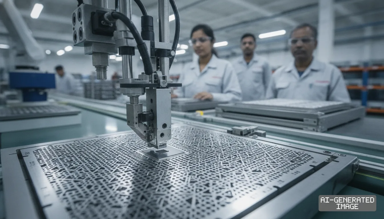
Micronex Technology said Oct. 5 it is constructing an 800 million rupee ($9.5 million) semiconductor lead-frame manufacturing plant in Sanand, Gujarat, targeting an annual output of 500 million units.
The facility represents the first dedicated domestic supply source for lead frames in India. Most packaging facilities operating in the country currently import these critical metal skeletons from Taiwan, China and Japan.
The initial outlay covers land, stamping equipment and plating lines in the GIDC Sanand Industrial Estate. The investment accounts for an initial fraction of Gujarat's 1.4 trillion rupee ($16.7 billion) committed semiconductor capital pool.
Lead frames are thin metal lattices that physically support a semiconductor die and conduct electrical signals to an external printed circuit board. Modern outsourced semiconductor assembly and test plants cannot package legacy chips without them.
Micronex will produce copper-alloy lead frames ranging from 0.1 millimeters to 0.25 millimeters in thickness. That dimension matches the thickness of standard industrial sheet stock used in power and automotive electronics.
The manufacturing process combines high-speed progressive mechanical stamping with chemical plating. The Sanand factory will integrate in-house silver-spot and nickel-plating lines to ensure solderability and wire-bond integrity, the company said.
The plant will supply packaging facilities handling high-current applications. Initial production runs will focus exclusively on power discrete devices and automotive microcontrollers before expanding into consumer electronics and telecommunications hardware, the company said.
Sanand is rapidly developing into India's primary outsourced semiconductor assembly and test cluster. Housing raw material suppliers alongside packaging plants reduces logistics delays and currency risks for local assemblers.
Kaynes Semicon signed a memorandum of understanding with Micronex in September to evaluate domestic lead-frame sourcing. The pact creates a commercial offload channel within the same industrial park.
Kaynes Semicon is ramping a 33 billion rupee ($393 million) packaging plant in Sanand. That facility operates a rated capacity of six million chips per day across power electronics and automotive lines.
Local component availability allows domestic packagers to adjust tooling schedules and custom lead dimensions rapidly. Importing customized stamping frames typically requires transit windows of three to six weeks.
The Sanand industrial corridor also hosts advanced assembly sites from global memory and power device manufacturers. Micron Technology is constructing a $2.75 billion assembly and test facility nearby.
Micron's Sanand plant processes dynamic random-access memory and flash memory packages. While memory modules primarily use multi-layer printed substrates rather than stamped frames, shared infrastructure lowers general supply costs across the park.
CG Semi, a joint venture led by CG Power, is establishing a 76 billion rupee ($905 million) packaging facility in the same manufacturing hub. That operation will assemble legacy power and automotive chips that rely directly on lead frames.
Rehan Mansuri founded Ahmedabad-based Micronex to address shortages in basic semiconductor hardware inputs. Mansuri's family previously established and operates seven plastic recycling facilities across India.
Domestic manufacturing of stamped frames shields Indian OSAT operations from supply chain disruptions. Stamping lead frames inside Gujarat eliminates import freight expenses and port customs clearance steps.
The company has started site construction at the Sanand estate. Structural fabrication of the main production hall and foundation work for heavy stamping machinery are underway, the company said.
Micronex plans to commission the factory and begin commercial shipments by May 2027. The plant will create approximately 250 direct manufacturing and engineering jobs once operating at full scale, the company said.
The company plans to submit a formal application under the central government's India Semiconductor Mission 2.0 program. The program provides capital support for semiconductor sub-component and material manufacturing projects.
India Semiconductor Mission 2.0 expands fiscal subsidies beyond front-end wafer fabs and large packaging units. The updated program offers central grants covering up to 50% of eligible project capital costs for component suppliers.
The state government of Gujarat provides an additional fiscal incentive through its state electronics policy. Qualified projects can receive a top-up subsidy covering 20% of capital expenditure from state funds.
The Gujarat State Electronics Mission has not published the subsidy disbursal schedule for the plant, and neither party has disclosed the minimum volume commitments under the Kaynes Semicon memorandum of understanding.
Commercial production trials for customer qualification are scheduled to begin in the first quarter of 2027 ahead of full-scale deliveries.
Impact map
How this development propagates across the region and out to global buyers.
| Event | Korea | China | Japan | Global impact |
|---|---|---|---|---|
| Micronex Sanand lead-frame fab | no direct exposure, local suppliers dominate Korean OSAT lead-frame demand | domestic stamping exporters face gradual displacement in Indian packaging supply lines | precision alloy and stamping tool makers gain downstream equipment demand | Indian OSAT cluster deepens self-sufficiency for discrete power and automotive packaging |
In this story
- Companies
- Micronex Technology
- Exposed
- Kaynes TechnologyMicron TechnologyCG Power
- Policy
- Subsidies
- Impact
- Supply ChainCapexCost Structure
Track every Subsidies development →
Related briefings
- Tokyo Electron Deploys Cryogenic Etch Systems to Challenge US Grip on 3D NAND Also on Micron Technology, Cost Structure
- TSMC Urges HBM Makers to Adopt X-Ray Friendly Chip Design for Advanced Packaging Also on Micron Technology, Cost Structure
- High-purity hydrogen peroxide supply chains face regional bottlenecks across East Asian fabs [90 characters] Also on Micron Technology, Cost Structure
- Micron Cuts DRAM Lead of SK hynix to One Point on HBM Demand Also on Micron Technology
Sources
Reporting
Confidence: medium — how we grade this
The documents behind this briefing are linked above. East Asia Brief produces its English text with AI assistance under human editorial review, and does not translate or republish other outlets' articles. See our methodology and AI policy. Spotted an error? Tell us.
The Morning Brief
What changed in Korean, Chinese and Japanese industry overnight — and what it means for your supply chain. One email, weekday mornings, US time. Free.
The Morning Brief is in preparation. Leave your address and we will write to you once — when the first issue is ready. Nothing before that.