TOPPAN and Broadcom open Singapore plant for AI substrates
The 95,000-square-meter facility in Jurong marks TOPPAN’s first overseas FC-BGA base and Broadcom’s push to secure critical packaging materials for high-speed AI processors.
Advanced Substrate Technologies opened Singapore's first production facility for advanced semiconductor packaging substrates on Sept. 29, 2026, targeting commercial shipments for artificial intelligence processors and network switches late this year.
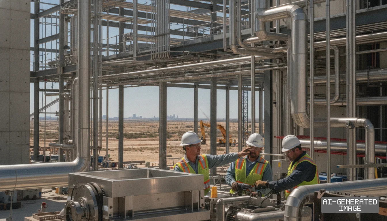
The manufacturing site spans 95,000 square meters in the Jurong Lake District. It represents the first overseas production facility for high-end packaging substrates built by Japanese materials group TOPPAN Holdings.
The venture aims to relieve chronic bottlenecks in advanced packaging. High-performance computing accelerators and networking processors require large-body flip-chip ball grid array, or FC-BGA, substrates to transfer signals between silicon dies and system circuit boards.
Substrate shortages during the pandemic capped production of complex logic chips across global foundries. The new Singapore facility provides dedicated manufacturing capacity for custom AI accelerators and high-bandwidth switches designed by Broadcom.
Singapore is expanding its semiconductor cluster from wafer fabrication and assembly into high-value component materials. The Southeast Asian hub already accounts for roughly 10% of global semiconductor output and 20% of semiconductor equipment manufacturing.
The Jurong plant complements TOPPAN’s primary substrate manufacturing base in Niigata, Japan. Dual-site production protects key customers against natural disasters and regional trade disruptions, company executives said during the opening ceremony.
TOPPAN plans to expand its global FC-BGA manufacturing capacity by 2.5 times by fiscal 2027 compared with fiscal 2022 levels. The Singapore site will contribute a major share of that incremental volume.
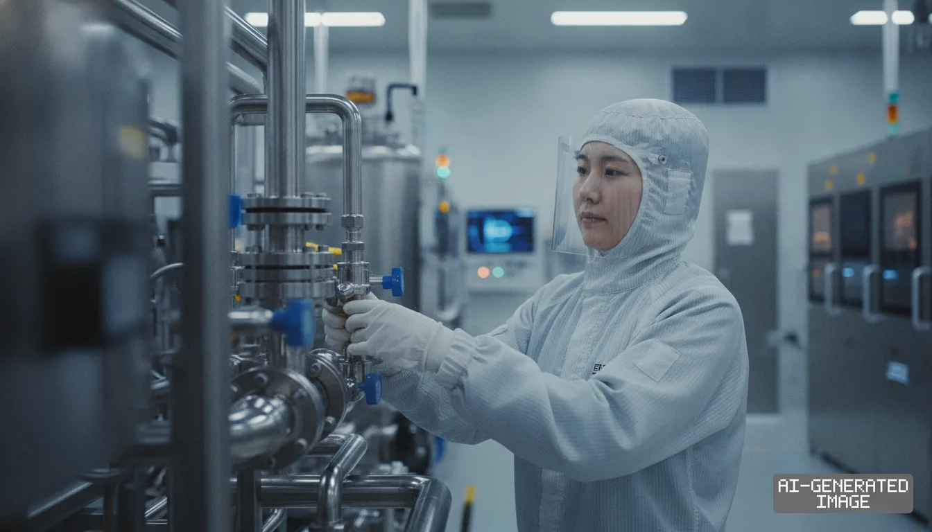
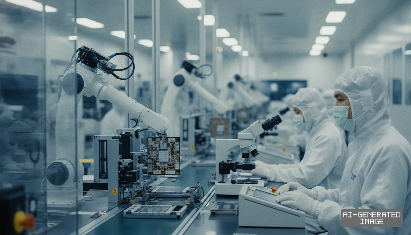
The factory integrates automated cleanroom lines to manufacture substrates featuring high layer counts and surface areas exceeding 100 millimeters by 100 millimeters. Those dimensions are required to package multi-die processor clusters.
Engineering teams at the site have begun pilot qualification runs on dedicated test lines. The company hired more than 200 technical personnel during construction and plans to increase total headcount past 330 specialists.
Initial engineering recruits completed technical training at TOPPAN’s Niigata facilities before commissioning machinery in Singapore. The site will also conduct research and development alongside local research institutes to develop thinner dielectric layers.
Rising demand for generative AI infrastructure has pushed packaging capacity to its limits worldwide. Server clusters running thousands of interconnected chips require specialized substrates that preserve signal integrity across high data transfer speeds.
Broadcom formed the joint venture to secure proprietary allocation of these multi-layer components. Securing dedicated lines prevents delivery delays for its Tomahawk network switches and custom application-specific integrated circuits.
Substrate delivery lead times stretched past 40 weeks during previous peak demand cycles. Broadcom executives sought direct equity participation in substrate manufacturing lines to eliminate similar procurement risks in future product rollouts.
The investment also advances Singapore’s long-term plan to anchor advanced chip packaging within its borders. The country has offered infrastructure support through the Economic Development Board to attract capital-intensive front-end and back-end projects.
The opening followed the Sept. 28 inauguration of a $7.8 billion wafer fab operated by Vanguard International Semiconductor and NXP Semiconductors in Singapore. That adjacent project will produce 300-millimeter power and analog chips.
Adding domestic substrate production gives chip designers in Singapore access to local fabrication, packaging and substrate materials. It also reduces transit times for materials moving between Southeast Asian assembly plants and testing centers.
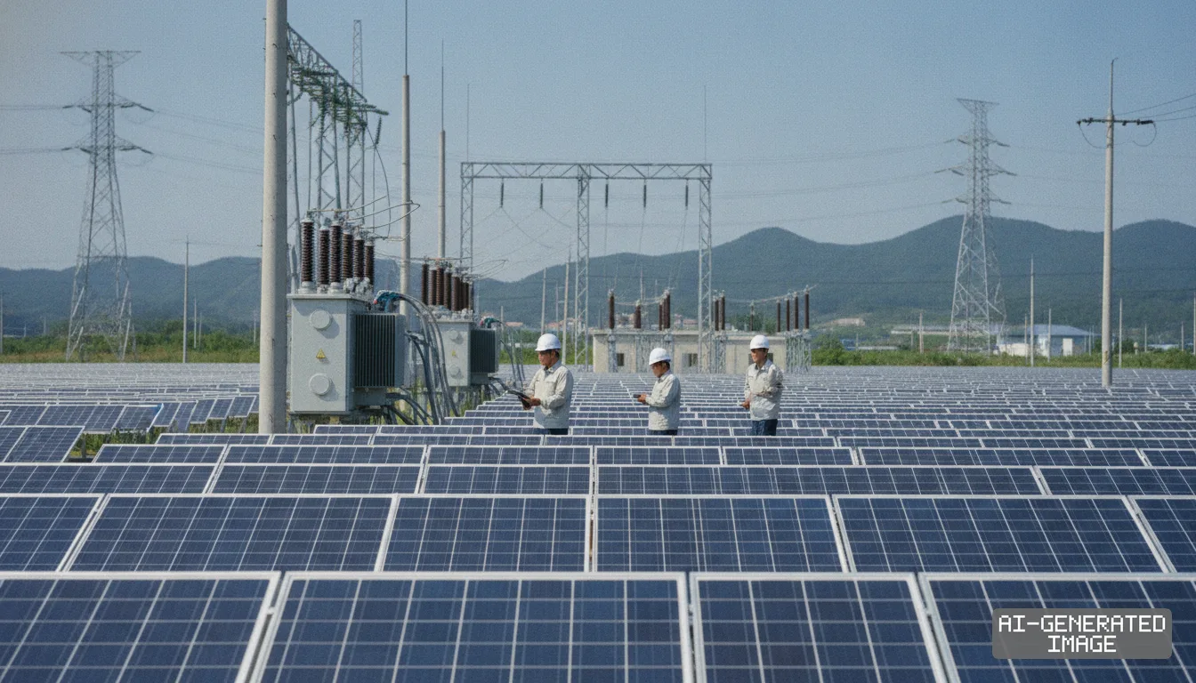
The facility incorporates rooftop solar arrays and closed-loop wastewater recycling equipment. The environmental systems comply with Singapore’s industrial sustainability mandates for high-power semiconductor facilities.
Advanced Substrate Technologies said commercial high-volume manufacturing will begin before the end of 2026. Output from initial production lines will ship directly to advanced packaging facilities across Asia.
The joint venture partners did not disclose the total capital expenditure for the Jurong facility, and official corporate filings did not confirm Japanese media estimates of 50 billion yen ($340 million).
Impact map
How this development propagates across the region and out to global buyers.
| Event | Korea | China | Japan | Global impact |
|---|---|---|---|---|
| Singapore FC-BGA substrate launch | no direct capacity exposure, maintains domestic supply at Samsung Electro-Mechanics | limited access to high-end large-body FC-BGA lines due to packaging export constraints | TOPPAN expands base beyond Niigata toward 2.5x fiscal 2027 output target | Broadcom secures captive packaging components, easing AI switch supply risks |
In this story
- Companies
- TOPPAN HoldingsBroadcomAdvanced Substrate Technologies
- Tickers
- 7911.TAVGO
- Exposed
- NXP SemiconductorsVanguard International Semiconductor
- Policy
- SubsidiesEconomic Security
- Impact
- Supply ChainCapexCapacity
Track every Subsidies development → Track every Economic Security development →
Related briefings
- Vanguard and NXP open Singapore fab, weigh second chip plant Also on Vanguard International Semiconductor, NXP Semiconductors
- Rapidus begins trial runs on 2nm pilot line in Hokkaido ahead of 2027 target Also on Toppan Holdings
- Silicon interposer scaling drives foundry and OSAT shifts in 3.5D chiplets Also on Broadcom
- JCET expands automotive radar SiP packaging lines to capture ADAS sensor demand Also on NXP Semiconductors
Sources
Reporting
Confidence: medium — how we grade this
The documents behind this briefing are linked above. East Asia Brief produces its English text with AI assistance under human editorial review, and does not translate or republish other outlets' articles. See our methodology and AI policy. Spotted an error? Tell us.
The Morning Brief
What changed in Korean, Chinese and Japanese industry overnight — and what it means for your supply chain. One email, weekday mornings, US time. Free.
The Morning Brief is in preparation. Leave your address and we will write to you once — when the first issue is ready. Nothing before that.