Samsung begins building $4.5B Onyang advanced packaging fab
The 6 trillion won cleanroom build anchors a 46 trillion won program in Asan to ease global bottlenecks in artificial intelligence accelerator supply.
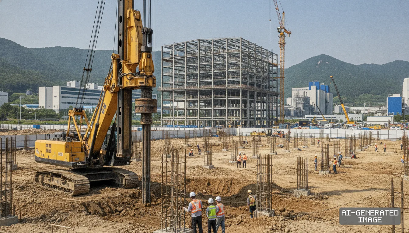
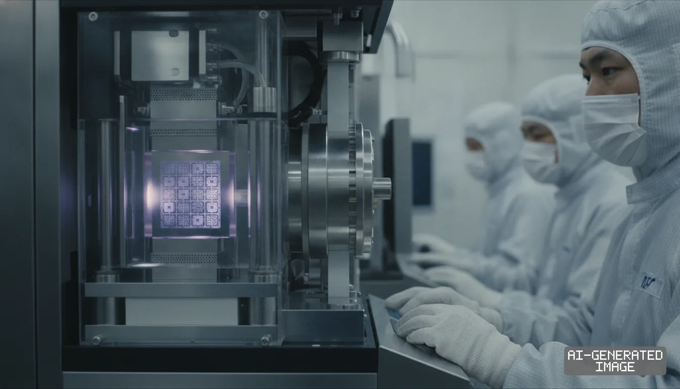
Samsung Electronics initiated foundation work Nov. 14 on a 6 trillion won ($4.5 billion) packaging line at its Onyang campus, expanding high-bandwidth memory assembly to counter persistent bottlenecks across global packaging capacity.
The building contract represents the physical core of a phased 46 trillion won ($34.5 billion) advanced packaging program at the site in Asan, South Korea. Equipment installations will account for roughly 40 trillion won, or 87% of the total capital expenditure, the company said.
The project adds 31,000 square meters of cleanroom floor space across three stories inside the new Line 5 facility. Once completed, total operating floor space at the Onyang campus will increase by 56% to 420,000 square meters, according to municipal planning records.
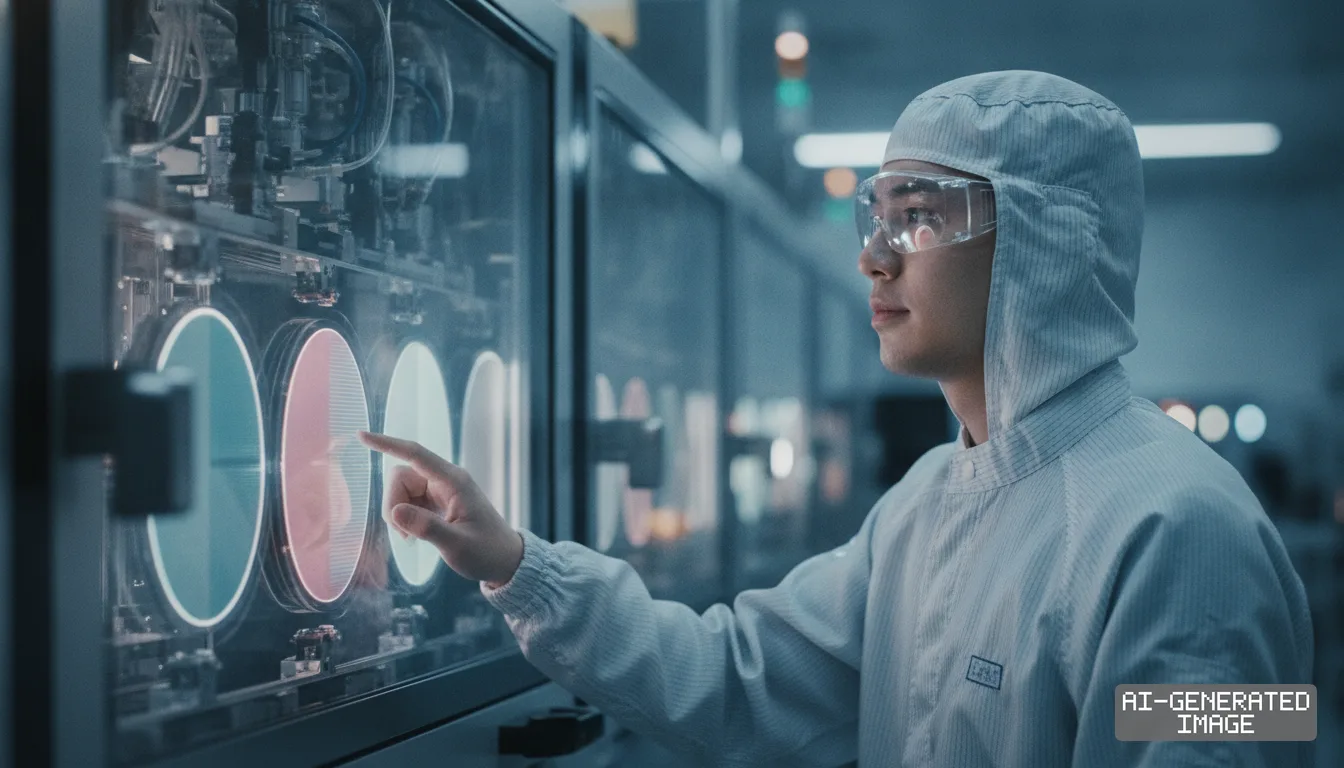
Samsung is directing the cleanroom expansion toward stacking and packaging next-generation high-bandwidth memory (HBM). The memory standard stacks dynamic random-access memory dies vertically, linking them through microscopic vertical channels called through-silicon vias to accelerate data delivery to artificial intelligence processors.
Advanced packaging has emerged as the central chokepoint in artificial intelligence hardware production. Pure-play foundry Taiwan Semiconductor Manufacturing Co. (TSMC) controls over 80% of global capacity in 2.5D advanced packaging, an integration method that places logic dies and memory stacks side by side on a shared silicon interposer.
That concentration has left server makers facing backlogs. Leading accelerator supplier Nvidia books virtually all its high-end graphic processor packaging through TSMC lines, where packaging turnaround backlogs have sustained customer lead times of 12 to 18 months.
Rival memory maker SK hynix supplies roughly 50% to 60% of high-bandwidth memory stacks bound for Nvidia accelerators, routing its processed memory cubes to TSMC for final substrate bonding. That arrangement splits manufacturing control across multiple independent contract fabricators.
Samsung is positioning the expanded Onyang campus to break that division by offering full turnkey integration. The turnkey model allows a single vendor to handle front-end logic fabrication, high-bandwidth memory die production and final 2.5D packaging within one consolidated operational chain.
The Onyang campus originally opened in late 1991 as a conventional backend facility dedicated to wire bonding, simple plastic encapsulation and final testing. The site is now being restructured into an advanced packaging hub capable of handling sub-micron interconnects and hybrid bonding.
Hybrid bonding joins copper pads directly without solder microbumps, preventing thermal throttling as memory stacks grow taller. Samsung plans to deploy the technique for 16-high HBM4 and HBM4E units targeted at next-generation data center processors.
Tight cleanroom availability at Samsung's Cheonan packaging site prompted the company to shift its new packaging lines to nearby Onyang. The Asan municipal government estimated the construction phase requires 3,400 site workers daily and will generate 700 permanent operations jobs upon commissioning.
Samsung advanced its target operational date for the Line 5 building by 12 months in response to tightening server build schedules. Initial cleanroom operations are scheduled to begin in June 2028.
The company targets commercial mass production at the facility for May 2029. That production schedule aligns with the anticipated volume transition toward HBM4E architectures among primary fabless accelerator designers.
The company has not disclosed the monthly wafer processing capacity or the target stack run rate for Line 5, and municipal planning filings do not specify the initial tool delivery schedule.
Impact map
How this development propagates across the region and out to global buyers.
| Event | Korea | China | Japan | Global impact |
|---|---|---|---|---|
| Onyang Line 5 packaging build | Samsung adds 31,000 m2 cleanroom to secure domestic HBM turnkey line | Domestic AI designers face persistent packaging bottlenecks under US export controls | Tool suppliers capture portion of 40 trillion won packaging equipment allocation | Relieves 2.5D packaging bottlenecks where TSMC controls over 80% share |
In this story
- Companies
- Samsung Electronics
- Tickers
- 005930.KS
- Exposed
- TSMCNvidiaSK hynix
- Impact
- CapexSupply ChainOrder Book
Related briefings
- Nvidia aligns TSMC and memory makers to ease 20% packaging shortfall Also on TSMC, Nvidia, SK hynix
- Samsung taps TSMC for custom HBM4 base dies in foundry shift Also on TSMC, Nvidia, SK hynix
- Micron taps TSMC for custom HBM4E memory, taking on SK hynix Also on TSMC, Nvidia, SK hynix
- Synopsys certifies TSMC A14 EDA flows and tapes out 64G UCIe Also on TSMC, Nvidia, SK hynix
Sources
Primary documents
Reporting
Confidence: high — how we grade this
The documents behind this briefing are linked above. East Asia Brief produces its English text with AI assistance under human editorial review, and does not translate or republish other outlets' articles. See our methodology and AI policy. Spotted an error? Tell us.
The Morning Brief
What changed in Korean, Chinese and Japanese industry overnight — and what it means for your supply chain. One email, weekday mornings, US time. Free.
The Morning Brief is in preparation. Leave your address and we will write to you once — when the first issue is ready. Nothing before that.