Samsung taps TSMC for custom HBM4 base dies in foundry shift
Nvidia requires suppliers to build custom NVHBM base dies on TSMC's 3-nanometer line, prompting Samsung to adopt a dual-track strategy alongside SK hynix's established foundry alliance.
Samsung Electronics established a dual-track manufacturing structure for customized HBM4 memory on Oct. 26, 2026, aligning with Taiwan Semiconductor Manufacturing Co. to satisfy client specifications for next-generation artificial intelligence accelerators.
The arrangement separates standard memory from bespoke products. Sixth-generation HBM4 stacks double the bus width to 2,048 bits and deliver up to 3.3 terabytes per second of bandwidth, compared with 1.2 terabytes on standard HBM3E.
Nvidia designed its custom NVHBM memory to transfer controller circuitry into the logic base die. The design cuts memory power consumption by 15% and frees up to 25% of compute die area on host processors.
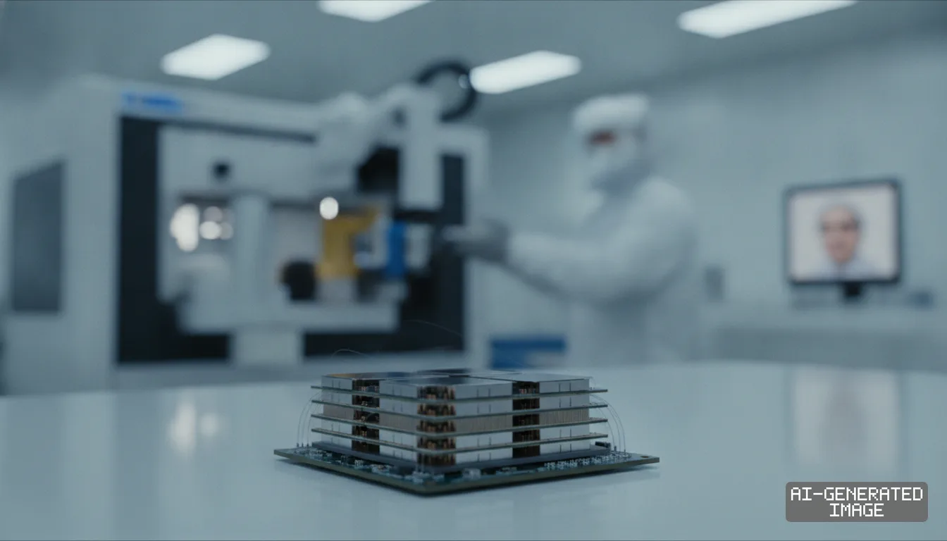
A base die — the foundation logic wafer that routes data between vertically stacked memory dies and the main processor — historically relied on standard DRAM manufacturing. Sixth-generation HBM4 shifts the component to advanced logic nodes.
Nvidia instructed all three memory partners to fabricate custom base dies using TSMC's three-nanometer node. Standardizing the manufacturing process eliminates timing discrepancies across suppliers, according to industry sources familiar with the guidelines.
Samsung Electronics will keep producing standard HBM4 and custom memory for AMD through its internal four-nanometer foundry. That turnkey service pairs 10-nanometer sixth-generation 1c DRAM with proprietary logic lines, the company said.
Samsung concentrates internal base-die fabrication on Line 17 at its Hwaseong campus and selected cleanroom lines at Pyeongtaek Fab 3. Tight logic capacity prompted company management to approve external sourcing for Nvidia's custom requirements.
TSMC controls roughly 85% of global advanced packaging and leading-edge logic fabrication. The Taiwanese foundry already manufactures Nvidia's primary graphics processor dies and manages wafer-level integration through its proprietary CoWoS packaging platform.
SK hynix built its advanced memory roadmap directly around TSMC. The Korean chipmaker signed an advanced packaging memorandum of understanding with TSMC in April 2024 to co-develop HBM4 stacks and system-in-package solutions.
SK hynix presented 16-layer 48-gigabyte HBM4 modules utilizing TSMC logic base dies at the TSMC OIP forum on Sept. 28. SK hynix currently accounts for more than 50% of global high-bandwidth memory shipments.
Micron Technology received identical production specifications from Nvidia for custom memory stacks. The Idaho chipmaker operates no commercial logic foundry, leaving it entirely dependent on TSMC for base-die fabrication and subsequent interposer attachment.
Directing every custom base die through TSMC concentrates production risks across global artificial intelligence hardware. TSMC's three-nanometer capacity remains tightly committed to mobile processors and accelerator compute tiles through late 2027.
Advanced packaging capacity creates an additional supply bottleneck. TSMC continues expanding its advanced packaging facilities across Taiwan, but lead times for specialized multi-die bonding equipment extend beyond nine months across Asian tool vendors.
Samsung's adoption of TSMC logic erodes a historic operational contrast with SK hynix. Both suppliers will now assemble custom memory on identical TSMC logic foundations, focusing competition on memory yields and thermal packaging efficiency.
Stacking methods remain distinct between the two South Korean manufacturers. SK hynix applies advanced mass reflow molded underfill, whereas Samsung uses advanced thermal compression non-conductive film before transitioning toward direct hybrid bonding.
Stacking 16 DRAM core dies creates severe thermal resistance inside accelerator modules. Direct copper-to-copper hybrid bonding eliminates intermediate microbumps to lower stack height, but processing costs remain substantially higher than conventional reflow assembly.
Samsung continues testing a two-nanometer gate-all-around foundry process as an alternative base-die channel. Company engineers are evaluating the node to support future custom memory if TSMC wafer allocation tightens further.
Hyperscale cloud operators including Amazon and Google develop proprietary custom accelerators that continue using standard memory architectures. That parallel market maintains volume demand for Samsung's single-roof memory and foundry manufacturing service.
Splitting fabrication across external foundries alters memory cost models. Memory suppliers must purchase finished three-nanometer logic wafers from TSMC at market rates, compressing operating margins relative to fully integrated in-house manufacturing.
Nvidia holds $279 billion in multi-year semiconductor purchase commitments across its foundry and memory supply chain. Securing dual memory vendors for NVHBM protects production targets for upcoming Vera Rubin computing platforms.
Commercial delivery and volume ramp of artificial intelligence systems featuring custom HBM4 memory will begin in the third quarter of 2027. Memory suppliers complete final engineering silicon validation by Dec. 15.
Samsung Electronics and TSMC have not published a regulatory filing or formal commercial contract confirming the three-nanometer agreement. Neither firm has disclosed baseline yield targets or wafer allocation volumes.
Impact map
How this development propagates across the region and out to global buyers.
| Event | Korea | China | Japan | Global impact |
|---|---|---|---|---|
| custom HBM4 foundry realignment | Samsung and SK hynix both rely on TSMC 3nm logic for Nvidia NVHBM base dies | CXMT remains locked out of advanced 2.5D packaging and logic-memory integration | Tool suppliers including Disco and Tokyo Electron see packaging equipment demand expand | Nvidia secures dual-vendor HBM4 supply while TSMC consolidates advanced packaging control |
In this story
- Companies
- Samsung ElectronicsSK hynixTSMCNvidia
- Tickers
- 005930.KS000660.KS2330.TWNVDA
- Exposed
- AMDMicron Technology
- Impact
- Supply ChainCapexOrder Book
Related briefings
- Samsung narrows SK hynix HBM lead as HBM4 shipments expand Also on AMD, Micron Technology, TSMC
- TSMC raises 2nm wafer target to 120,000 units as orders surge Also on AMD, TSMC, Nvidia
- AMD weighs Samsung foundry alliance to ease reliance on TSMC Also on AMD, TSMC, Samsung Electronics
- South Korean substrate makers develop embedded silicon bridges for AI chips Also on AMD, SK hynix
Sources
Reporting
Confidence: medium — how we grade this
The documents behind this briefing are linked above. East Asia Brief produces its English text with AI assistance under human editorial review, and does not translate or republish other outlets' articles. See our methodology and AI policy. Spotted an error? Tell us.
The Morning Brief
What changed in Korean, Chinese and Japanese industry overnight — and what it means for your supply chain. One email, weekday mornings, US time. Free.
The Morning Brief is in preparation. Leave your address and we will write to you once — when the first issue is ready. Nothing before that.