Tokyo Electron defends 3.7 trillion yen target as shares slip
First-half operating profit surged 67.2% to 506.78 billion yen, but equity sell-offs test the company's full-year 1.169 trillion yen operating forecast.
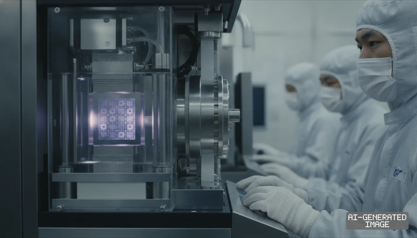
Tokyo Electron faced renewed investor scrutiny on Nov. 15, 2026, as chipmaker share pullbacks tested whether high-margin etch tools can sustain the equipment maker's record earnings pace.
The Tokyo-based company raised its full-year net sales forecast on Oct. 30 to a record 3.70 trillion yen ($24.2 billion), representing a 51% increase over the previous fiscal year.
Operating income for the fiscal year ending March 2027 is projected at 1.169 trillion yen, while the first half generated 506.78 billion yen, up 67.2% from a year earlier.
First-half revenue rose 41.3% to 1.67 trillion yen, accounting for roughly 45% of the company's full-year target as capital spending rebounded across major memory manufacturers.
Shares closed at 9,461 yen on the Tokyo Stock Exchange on Nov. 13, leaving the supplier trading at elevated multiples following a 5-for-1 stock split executed on Oct. 1.
The global wafer fab equipment market will reach approximately $160 billion in 2026 before expanding past $210 billion in 2027, the company projected in its latest industry forecast.
Tokyo Electron relies on advanced memory fabrication to drive its next growth phase as leading memory producers accelerate migrations toward sub-10-nanometer DRAM and dense vertical NAND architectures.
In DRAM processing, Tokyo Electron secured one new mass-production process of record for capacitor mask conductor etch on next-generation architectures, according to its Oct. 30 business presentation.
A process of record represents formal customer qualification to deploy a specific tool model in high-volume manufacturing lines, locking in recurring tool deliveries and spare parts revenue.
The company already holds an established market position in capacitor mold dielectric etch, using specialized plasma chambers to carve narrow support structures without wafer warping.
In NAND flash, memory producers face severe physical limitations as vertical layer counts surpass 300 and 400 tiers, demanding deep vertical holes etched at microscopic aspect ratios.
Conventional plasma etch processes generate excessive heat, slowing processing speeds and causing hole distortion when drilling through dozens of alternating oxide and nitride films.
Tokyo Electron developed cryogenic etch technology to address this bottleneck, chilling silicon wafers to extreme sub-zero temperatures during halogen gas etching to accelerate chemical reaction rates.
The cryogenic method cuts process times while eliminating fluorocarbon residues, enabling memory makers to drill channel holes across 400 layers in single-step passes rather than multiple bonded stages.
Tokyo Electron reported steady order progress for cryogenic etch tools intended for volume manufacturing in its investor guide released Nov. 9.
The company links its etch portfolio to lithography track equipment, where Tokyo Electron retains a dominant share exceeding 90% in coater-developers paired with extreme ultraviolet scanners.
The transition to high numerical aperture extreme ultraviolet tools forces chipmakers to adopt thinner photoresist films, requiring highly selective dry etch chemistries to pattern delicate circuit lines.
Beyond memory, advanced packaging demand continues to expand as artificial intelligence accelerators shift to multi-die integration architectures requiring vertical silicon interconnects and micro-bumps.
Shipments of deep trench capacitor high-k atomic layer deposition tools will exceed 200 units annually across both fiscal 2027 and fiscal 2028, the company projected.
Export licensing regulations imposed by Japan and the United States continue to restrict shipments of advanced lithography and etch tools to semiconductor fabrication facilities in China.
Mature-node tool shipments to Chinese domestic producers had supported equipment revenues over the prior two years, making leading-edge node expansion in other regions critical to maintaining margins.
Tokyo Electron scheduled payment of an interim dividend of 415 yen per share, calculated on a pre-split basis, for distribution on Nov. 27.
The company announced Nov. 12 that it will establish a Device Integration Strategy Unit within its Corporate Innovation Division, taking effect Dec. 1 to align packaging and etch development.
Tokyo Electron did not disclose the unit volume or contract value of its cryogenic etch orders, and the company has not published customer-specific terms for its DRAM mask etch deployment.
Tool deliveries under the newly secured DRAM conductor etch process of record will begin during the fiscal fourth quarter ending March 31, 2027.
Impact map
How this development propagates across the region and out to global buyers.
| Event | Korea | China | Japan | Global impact |
|---|---|---|---|---|
| Advanced etch adoption | Samsung and SK hynix evaluate cryogenic tools for 400-layer NAND lines | export controls block leading-edge etch tool deliveries to domestic fabs | Tokyo Electron maintains >90% EUV track share while scaling etch orders | wafer fab equipment spending projected to pass $210B in 2027 |
In this story
- Companies
- Tokyo Electron
- Tickers
- 8035.T
- Policy
- Export Controls
- Impact
- Order BookCapexValuation
Track every Export Controls development →
Related briefings
- TSMC steadies at 21x earnings with 73% share of foundry spending Also on Valuation
- SK hynix Evaluates Solidigm US IPO Amid Governance Scrutiny Also on Valuation
- Tokyo Electron nears 1 trillion yen profit on memory capex Also on Tokyo Electron, Export Controls, Order Book
- Naura and SMEE Accelerate Domestic Tool Shipments to Chinese Fabs Also on Tokyo Electron, Export Controls, Order Book
Sources
Reporting
Confidence: medium — how we grade this
The documents behind this briefing are linked above. East Asia Brief produces its English text with AI assistance under human editorial review, and does not translate or republish other outlets' articles. See our methodology and AI policy. Spotted an error? Tell us.
The Morning Brief
What changed in Korean, Chinese and Japanese industry overnight — and what it means for your supply chain. One email, weekday mornings, US time. Free.
The Morning Brief is in preparation. Leave your address and we will write to you once — when the first issue is ready. Nothing before that.