Samsung allocates Taylor Fab 2 for advanced HBM base dies
Advance commitments reportedly reserve the 2.7-million-square-foot plant for 2nm logic dies that integrate with Korean DRAM to challenge TSMC's packaging grip.
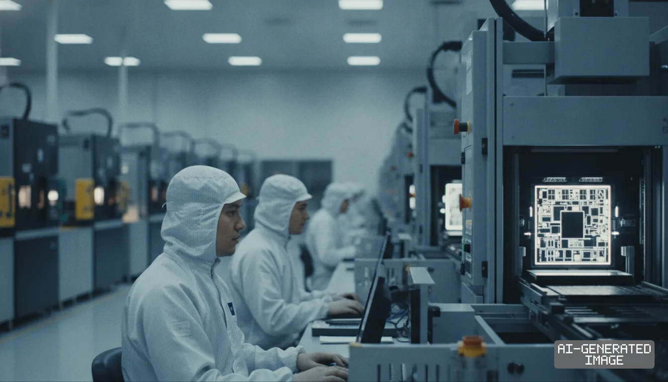
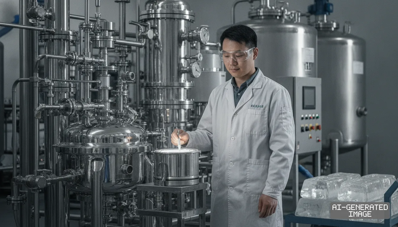
Samsung Electronics decided to designate its second Taylor, Texas fabrication plant entirely for advanced memory base dies, South Korea's Maeil Business Newspaper reported on Nov. 3, 2026.
The facility, known as Taylor Fab 2, spans approximately 2.7 million square feet (about 250,000 square meters). That floor plan makes the second building roughly 1.5 times the size of Samsung's first Taylor plant.
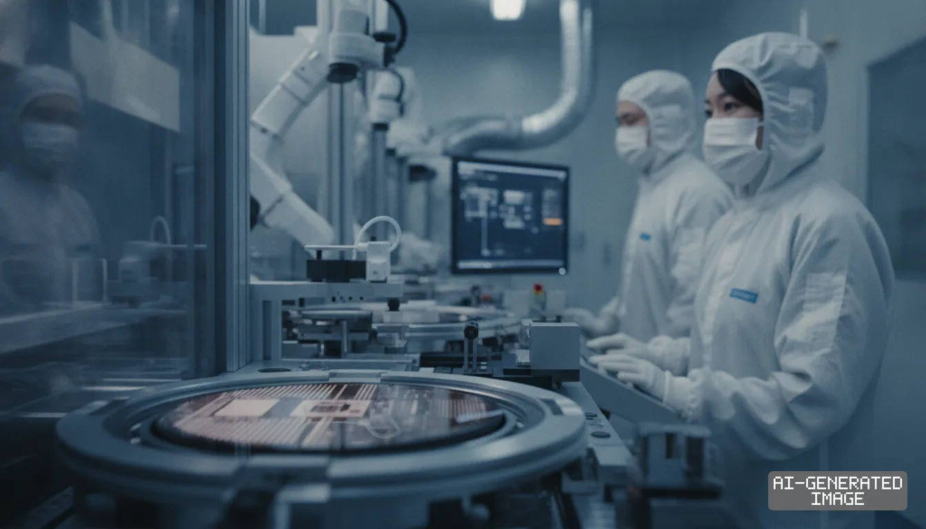
The plant will deploy Samsung's 2-nanometer foundry process to produce logic base dies for high-bandwidth memory (HBM). Advance production commitments reportedly absorb 100% of the facility's projected manufacturing capacity.
Advanced Micro Devices accounts for the vast majority of the facility's committed volume, according to the report. Nvidia reserved the remaining share, leaving the second Taylor plant with zero unassigned capacity.
A base die serves as the physical and electrical foundation of an HBM stack. It routes data signals between vertical stacks of dynamic random-access memory (DRAM) and the central processor.
Earlier generations of high-bandwidth memory used standard memory manufacturing processes for the base die. Starting with the HBM4 generation, memory makers must switch to advanced logic nodes to sustain high data throughput.
Under the reported manufacturing structure, Samsung Foundry will produce the 2nm logic base dies in Texas. Samsung will then bond those components with core DRAM wafers fabricated at its memory lines in South Korea.
The bonded memory cubes will then ship to customers for system-level integration. The arrangement enables American chip designers to source logic silicon domestically while relying on South Korean memory wafer manufacturing.
The dedicated allocation represents a direct challenge to Taiwan Semiconductor Manufacturing Co., known as TSMC. TSMC currently manufactures the dominant share of advanced logic base dies and accelerator silicon globally.
TSMC also controls the market for Chip-on-Wafer-on-Substrate (CoWoS) packaging, an advanced packaging method that connects memory stacks directly to processing units on a silicon interposer.
Nvidia has urged memory suppliers to manufacture next-generation HBM base dies on TSMC's 3nm foundry line. That approach forces memory suppliers to synchronize production schedules with TSMC's manufacturing timeline.
AMD has sought dedicated foundry capacity to bypass production constraints across TSMC's packaging network. Sourcing base dies directly from Samsung provides AMD with an alternative supply channel independent of TSMC.
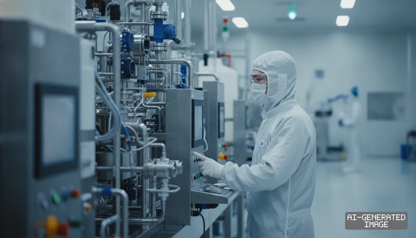
Samsung operates both contract foundry lines and high-volume DRAM fabrication plants. That corporate structure enables Samsung to market turnkey HBM manufacturing, handling logic fabrication, DRAM bonding and packaging internally.
Samsung previously manufactured 4nm base dies for HBM4 components supplied to Nvidia accelerator systems. That qualification milestone in early 2025 enabled Samsung to rebuild its share against SK hynix during 2026.
The broader Taylor site covers 1,268 acres, providing infrastructure room for up to 10 semiconductor plants. Samsung dedicated its first Taylor facility to computing chips, securing Tesla as an anchor customer for vehicle processors.
Samsung did not announce the customer allocation through regulatory disclosure channels. When asked about the report, a Samsung spokesperson said the company cannot confirm customer-related details.
In its third-quarter earnings release on Oct. 29, Samsung confirmed that its contract foundry business targets revenue growth led by 2nm nodes. The company said new facilities in Taylor will strengthen global production.
Samsung also told investors that demand across manufacturing nodes below 8nm currently exceeds available capacity. The foundry division plans to begin volume manufacturing of second-generation 2nm mobile chips in late 2026.
Site preparation at the Taylor Fab 2 plot is complete, clearing the land for structural assembly. Full structural construction begins in November 2026, according to the Korean media report.
Samsung targets cleanroom equipment delivery for February 2029, the report said. The company plans to begin commercial mass production on the 2nm Taylor lines in 2030.
The report does not state binding contract valuations or minimum wafer take-or-pay commitments. Samsung has not published regulatory filings confirming customer supply contracts with AMD or Nvidia.
Samsung has not confirmed whether Taylor Fab 2 will produce memory base dies exclusively. The company has not published formal engineering timelines confirming the 2030 mass production target.
Civil engineering contractors in Williamson County, Texas, will begin pouring structural concrete footings before the end of November 2026.
Impact map
How this development propagates across the region and out to global buyers.
| Event | Korea | China | Japan | Global impact |
|---|---|---|---|---|
| Taylor Fab 2 base die allocation | Samsung links Texas 2nm base dies to domestic DRAM fabs in Pyeongtaek | Domestic memory makers remain blocked from advanced 2nm logic base die production | Equipment vendors Tokyo Electron and Canon see extended tool delivery timelines into 2029 | AMD and Nvidia diversify advanced logic packaging away from single-source TSMC lines |
In this story
- Companies
- Samsung Electronics
- Tickers
- 005930.KS
- Exposed
- Advanced Micro DevicesNvidiaTaiwan Semiconductor Manufacturing Co.
- Impact
- CapexSupply Chain
Related briefings
- TSMC prepares to raise CoWoS packaging prices by up to 20% Also on Advanced Micro Devices, Taiwan Semiconductor Manufacturing Co., Nvidia
- GlobalFoundries signs $2 billion TSMC chip interposer deal Also on Advanced Micro Devices, Taiwan Semiconductor Manufacturing Co., Nvidia
- TSMC widens CoWoS supply chain with $2 billion US interposer deal Also on Advanced Micro Devices, Taiwan Semiconductor Manufacturing Co., Nvidia
- TSMC weighs Texas foundry campus to expand US chip capacity Also on Advanced Micro Devices, Taiwan Semiconductor Manufacturing Co., Nvidia
Sources
Reporting
Confidence: medium — how we grade this
The documents behind this briefing are linked above. East Asia Brief produces its English text with AI assistance under human editorial review, and does not translate or republish other outlets' articles. See our methodology and AI policy. Spotted an error? Tell us.
The Morning Brief
What changed in Korean, Chinese and Japanese industry overnight — and what it means for your supply chain. One email, weekday mornings, US time. Free.
The Morning Brief is in preparation. Leave your address and we will write to you once — when the first issue is ready. Nothing before that.