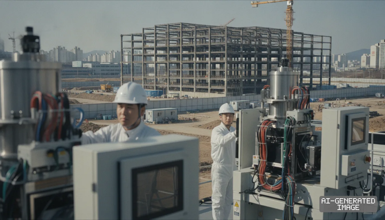
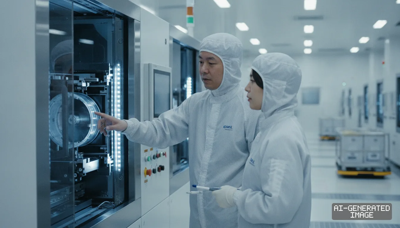
TSMC widens High-NA EUV alliance to build 12-inch photomasks by 2031
The foundry expanded supplier partnerships on Sept. 10 to establish larger reticle formats with ASML, targeting a 40% scanner productivity boost for artificial intelligence chips.

Taiwan Semiconductor Manufacturing Company broadened supply-chain partnerships on Sept. 10 to establish 12-inch photomasks for High-NA extreme ultraviolet lithography, targeting exposure bottlenecks in large artificial intelligence processors.
The initiative addresses optical limits in next-generation lithography scanners produced by ASML Holding. Moving from four-decade-old 6-inch masks to 12-inch plates will increase High-NA scanner productivity by about 40%, ASML said.
High-NA machines use a 0.55 numerical aperture lens that splits the exposure field in half, down to 26 by 16.5 millimeters. That optical reduction forces foundries to stitch two separate exposures together for 800-square-millimeter processors.
Stitching cuts scanner throughput and raises the risk of alignment defects at the die boundary. Larger photomasks eliminate the split-field constraint by doubling the reticle surface, enabling single-exposure patterning on giant accelerator dies.
Conventional 0.33 numerical aperture EUV scanners employ four-fold optical reduction across both axes to cover a 26 by 33 millimeter field. High-NA tools introduce anamorphic optics with eight-fold vertical reduction, cutting the effective exposure area by 50%.
TSMC plans to begin high-volume manufacturing with High-NA systems in 2030, using standard 6-inch masks first. The foundry expects the count of critical layers requiring High-NA exposure to multiply as transistor architectures grow denser.
The foundry deepened its partnership on Sept. 10 following formal agreements reached ahead of the SPIE BACUS Conference. ASML Chief Executive Christophe Fouquet said the shift will allow the industry to meet demand for faster processors.
TSMC Chairman and Chief Executive C.C. Wei said complex manufacturing hurdles require joint efforts across the value chain. Uniting suppliers lowers adoption barriers and makes advanced solutions accessible at commercial scale, Wei said.
Samsung Electronics joined the 12-inch initiative alongside TSMC and ASML, seeking to protect its memory roadmap. The South Korean manufacturer scheduled High-NA EUV adoption for high-volume dynamic random-access memory production by 2028.
Intel is also coordinating on the 12-inch specification after deploying early High-NA tools. Intel Foundry processed more than one million wafers on High-NA equipment for development and select layers of its Panther Lake client processors.
Early production at Intel demonstrated that stitching client dies is technically viable but operationally expensive. Expanding reticle dimensions removes that manufacturing penalty for enterprise graphics processing units that exceed single-field limits.
Substrate suppliers face retooling across their entire quartz blank manufacturing lines. Japan's HOYA and AGC, which control over 80% of global EUV mask blank production, are aligning development programs with the new dimensions.
Fabricating 12-inch mask blanks requires maintaining defect-free multilayer molybdenum and silicon coatings over an area four times larger than current substrates. Thermal expansion tolerances must remain within sub-nanometer thresholds during exposure.
The transition also requires redesigning protective pellicles — ultra-thin membranes mounted over masks to block airborne particles — to withstand high-power EUV beams across a doubled surface area without sagging or thermal warping.
Inspection toolmakers must re-engineer optical and electron-beam defect scanners to handle the heavier quartz plates. Lasertec and KLA need wider translation stages and upgraded vacuum chucks to hold larger reticles flat during inspection.
Photomask transport automation requires completely new handling pods and fab stockers. Mask carrier manufacturer Gudeng Precision Industrial saw its High-NA carrier certified by ASML as July revenue surged 71.69% year-over-year on front-opening unified pod demand.
Automated material handling systems across leading-edge fabs must be redesigned to accommodate the increased footprint of 12-inch mask pods. Foundry cleanroom bays will require dedicated overhead hoist transport tracks for reticle distribution.
Foundries have diverged in their operational timing for High-NA adoption because of tool costs exceeding $350 million per scanner. TSMC chose to extend 0.33 numerical aperture low-NA EUV through its 1.4-nanometer node generation.
TSMC concluded that low-NA multi-patterning remains more economical than early High-NA adoption through 2029. Introducing High-NA in 2030 allows the company to amortize mature tools before taking on high capital costs.
Samsung moved its timeline earlier to secure patterning margins on sub-10-nanometer memory architectures. Applying 0.55 numerical aperture scanners to DRAM in 2028 aims to reduce mask counts on dense capacitor layers.
The coordinated photomask project reflects memory and logic rivals setting aside competitive frictions to avoid costly custom standards. A shared format ensures toolmakers develop one equipment generation rather than competing proprietary platforms.
The alliance mirrors previous joint efforts that established EUV lithography after an industry attempt to transition to 450-millimeter silicon wafers collapsed. Tool vendors refused to fund wafer scaling without guaranteed multi-foundry procurement commitments.
By establishing an open specification, TSMC and ASML aim to distribute research costs across materials providers, mask shops and diagnostic vendors. That shared investment model mitigates execution risk across the lithography supply chain.
The initiative targets establishing a 12-inch photomask pilot line by 2031. System developers expect to achieve full lithography tool readiness for commercial advanced-node manufacturing lines by 2033.
Neither TSMC nor ASML disclosed the total capital expenditure budgeted for the pilot line. The partners have also not settled whether the final physical format will measure six by 12 inches or 12 by 12 inches.
Supply-chain working groups will present preliminary reticle specifications and mechanical handling guidelines during upcoming technical committee sessions at the SPIE Advanced Lithography conference.
Impact map
How this development propagates across the region and out to global buyers.
| Event | Korea | China | Japan | Global impact |
|---|---|---|---|---|
| 12-inch High-NA EUV photomask initiative | Samsung deploys High-NA in DRAM by 2028, joins 12-inch mask platform | Domestic foundries locked out of 0.55-NA tools, widening logic node gap | HOYA and AGC retool blank lines; Lasertec upgrades defect stages | AI accelerator dies avoid half-field stitching, boosting scanner throughput ~40% |
In this story
- Companies
- TSMCASML
- Tickers
- 2330.TWASML
- Exposed
- Samsung ElectronicsIntelHOYAAGCGudeng Precision Industrial
- Policy
- Economic Security
- Impact
- CapexSupply ChainPricing
Track every Economic Security development →
Related briefings
- Japan mask blank makers qualify High-NA EUV substrates for sub-2nm chips Also on Intel, ASML, TSMC
- Japanese photoresist makers validate metal oxide resist lines for High-NA EUV chipmaking Also on Intel, ASML, TSMC
- Tokyo Electron qualifies BSPDN coater-developer tracks for sub-2nm fabs Also on Intel, ASML, TSMC
- South Korea funds advanced chip packaging and backside power pilot lines Also on Intel, TSMC, Samsung Electronics
Sources
Reporting
Confidence: medium — how we grade this
The documents behind this briefing are linked above. East Asia Brief produces its English text with AI assistance under human editorial review, and does not translate or republish other outlets' articles. See our methodology and AI policy. Spotted an error? Tell us.
The Morning Brief
What changed in Korean, Chinese and Japanese industry overnight — and what it means for your supply chain. One email, weekday mornings, US time. Free.
The first issue goes out shortly. Sign up now and you will not miss it.