TSMC warns AI cannot solve physical barriers for 1.4nm chips
Co-Chief Operating Officer Y.J. Mii warns that automated design tools cannot bypass physical manufacturing limits as the foundry prepares its 1.4-nanometer node for 2028 volume production.
Taiwan Semiconductor Manufacturing Co. Co-Chief Operating Officer Y.J. Mii warned Sept. 19 that artificial intelligence cannot overcome the physical manufacturing barriers required to produce 1.4-nanometer chips.
The foundry's next-generation 1.4-nanometer process, designated A14, targets a 15% speed improvement or a 30% reduction in power consumption compared to its earlier 2-nanometer node. TSMC plans to initiate risk production on the technology in 2027.
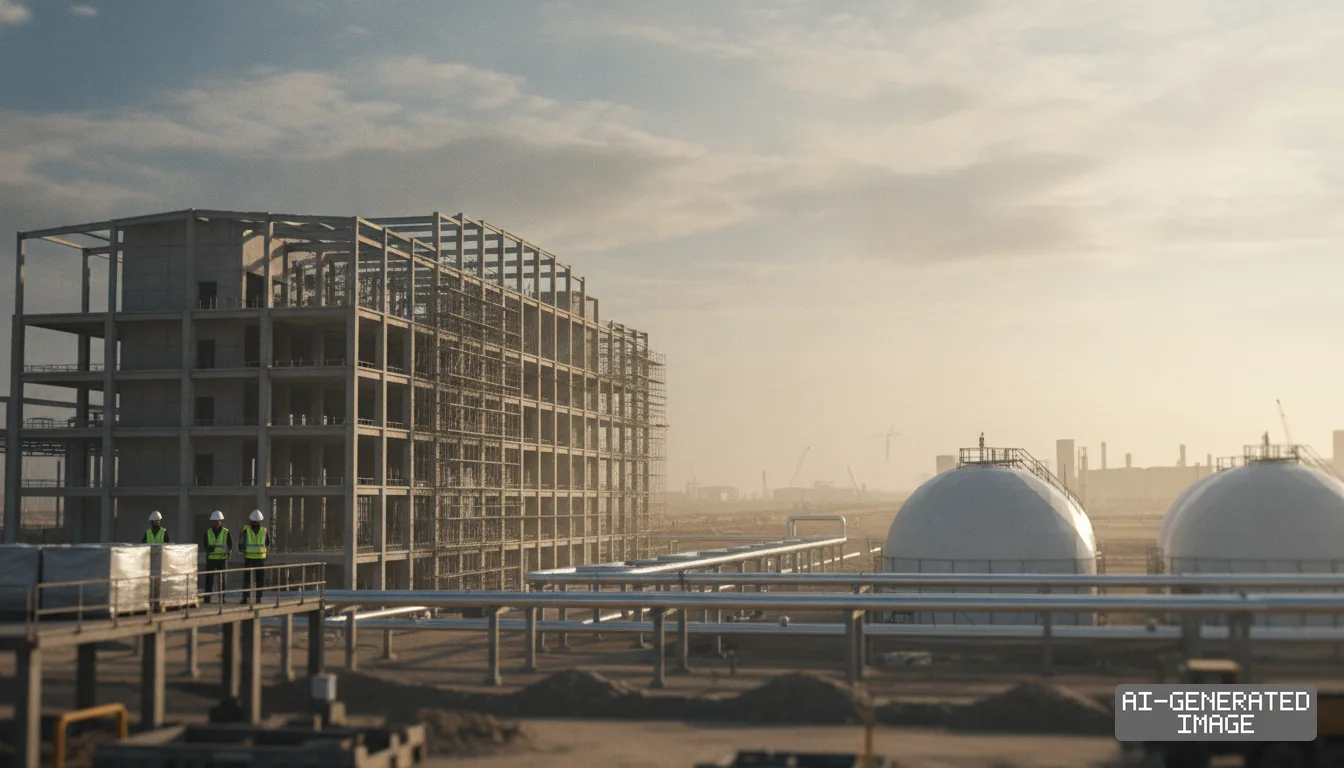
Taiwan's National Development Council approved a 104.19-hectare expansion for TSMC at Longtan Science Park on Sept. 17. The NT$95.63 billion ($2.99 billion) infrastructure project accommodates future angstrom-class fabrication facilities.
AI functions like a three-year-old superhero with extraordinary capabilities that cannot distinguish right from wrong, Mii said. The technology cannot anticipate the operational damage it might inflict on complex industrial projects, he added.
Mii drew a firm boundary between software design automation and physical wafer fabrication. AI tools handle well-defined tasks like code writing and basic layout mapping efficiently because input and output specifications are clearly structured, Mii said.
Commercial microprocessors routinely integrate tens of billions or hundreds of billions of transistors on a single die. Software algorithms optimize those massive component arrays far more rapidly than human engineering teams can execute manually, Mii said.
Fabricating physical hardware at atomic dimensions introduces problems where operational data does not yet exist, Mii said. When fundamental chemical processes and lithography tools cannot achieve required tolerances, machine learning models offer minimal assistance, he noted.
Developing angstrom-class technologies like A14 and sub-1-nanometer A10 requires exploring uncharted physical domains, Mii said. Algorithms cannot fabricate manufacturing steps that available equipment cannot physically produce on a silicon wafer, he emphasized.
Leading fabless design firms depend heavily on TSMC for frontier chip supply. Major customers Nvidia and Apple account for an estimated combined share of more than 35% of the foundry's total wafer revenues.
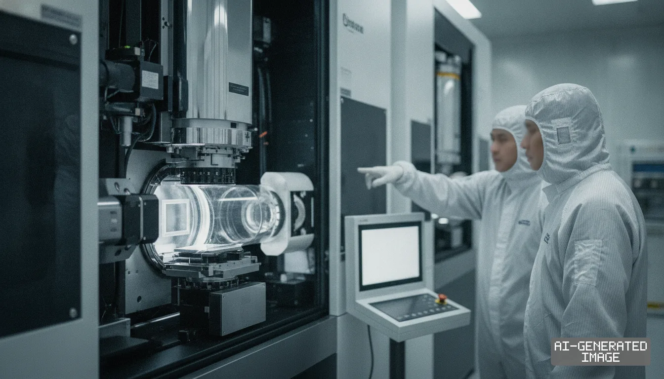
Next-generation node scaling requires high-numerical-aperture extreme ultraviolet lithography systems manufactured by ASML Holding. Those precision exposure tools cost roughly $380 million each and require entirely redesigned photoresists and wafer-handling architectures.
Mii also cautioned against feeding confidential research and development recipes into commercial AI platforms. Uncontrolled internal adoption risks leaking proprietary semiconductor formulas or corrupting sensitive proprietary design libraries, Mii said.
Recent data breaches involving external software environments like Hugging Face have raised alarms across the hardware supply chain. Industry leaders have pushed for stricter operational safeguards around automated coding and model testing.
TSMC strictly fences its internal process design kits and intellectual property libraries. The company prevents fabrication specialists from uploading proprietary recipes to external neural networks accessible by third parties.
Mii delivered his remarks during a technology panel at National Taiwan University, his alma mater. The discussion explored how advanced manufacturing teams must adapt to machine learning tools without abandoning disciplined engineering judgment.
Global foundries face escalating capital expenditure burdens as transistor gate dimensions shrink toward the atomic scale. Intel aims to deploy its competing 14A process in 2028, while Samsung Electronics pursues an equivalent 1.4-nanometer schedule.
Outfitting a commercial fabrication facility for sub-2-nanometer production now costs upwards of $20 billion. Unresolved manufacturing defects or delayed equipment deliveries can jeopardize the financial returns of an entire node cycle.
Critical process and capital allocations still demand human oversight, Mii said. Algorithms generate sharply diverging answers depending on whether questions focus on theoretical market potential or concrete capital returns, he explained.
Mii also acknowledged that managing international operations outside Taiwan presents steep managerial challenges. TSMC faces a shortage of senior managers capable of supervising overseas engineering personnel at facilities in the United States and Japan, Mii said.
TSMC has not published an official transcript or regulatory filing concerning Mii's remarks, which were delivered during an academic forum rather than an investor presentation.
TSMC is scheduled to begin risk production on the A14 node in 2027, followed by commercial volume production in 2028. Environmental reviews for the approved Longtan Science Park expansion site conclude in late 2028.
Impact map
How this development propagates across the region and out to global buyers.
| Event | Korea | China | Japan | Global impact |
|---|---|---|---|---|
| TSMC 1.4nm physical limits | Samsung faces identical High-NA EUV and atomic scaling barriers on SF1.4 | SMIC remains limited to multi-patterning DUV, trailing angstrom nodes by generations | Tokyo Electron and Canon supply advanced track and patterning tools for sub-2nm lines | Fabless customers Nvidia and Apple absorb higher wafer pricing as physical limits slow node gains |
In this story
- Companies
- Taiwan Semiconductor Manufacturing Co
- Tickers
- 2330.TWTSM
- Exposed
- NvidiaAppleIntelASML HoldingSamsung Electronics
- Policy
- Economic SecuritySubsidies
- Impact
- CapexSupply ChainOrder Book
Track every Economic Security development → Track every Subsidies development →
Related briefings
- TSMC revenue rises 53% on AI demand to record NT$514 billion Also on ASML Holding, Taiwan Semiconductor Manufacturing Co., Intel
- Naura and SMEE Accelerate Domestic Tool Shipments to Chinese Fabs Also on ASML Holding, Order Book
- TSMC Reaffirms 2028 Target for 1.4nm Chips at Taichung Fab Also on Apple, Taiwan Semiconductor Manufacturing Co, Intel
- TSMC sees 3nm revenue overtake 5nm node on surge in AI accelerators Also on Apple, Intel, Nvidia
Sources
Primary documents
Reporting
Confidence: high — how we grade this
The documents behind this briefing are linked above. East Asia Brief produces its English text with AI assistance under human editorial review, and does not translate or republish other outlets' articles. See our methodology and AI policy. Spotted an error? Tell us.
The Morning Brief
What changed in Korean, Chinese and Japanese industry overnight — and what it means for your supply chain. One email, weekday mornings, US time. Free.
The first issue goes out shortly. Sign up now and you will not miss it.