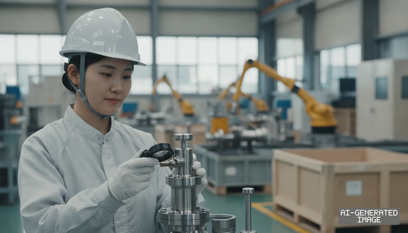
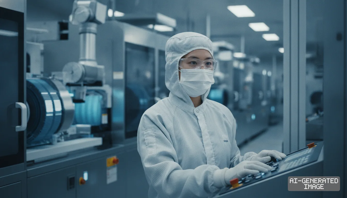
SK hynix starts $4 billion packaging plant in Indiana to feed US AI
The Purdue Research Park campus will open cleanrooms in October 2028 before starting mass production of next-generation high-bandwidth memory for American AI accelerator customers in late 2029.
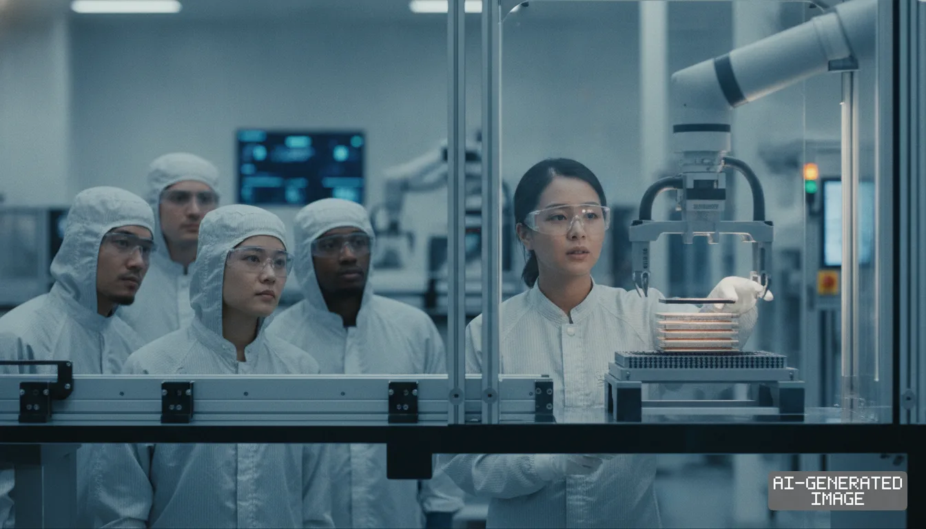
SK hynix advanced structural fabrication work Sept. 5 at its $4 billion advanced packaging site in West Lafayette, Indiana, following an Aug. 27 ceremonial groundbreaking.
The facility will process memory wafers shipped from South Korea into next-generation high-bandwidth memory modules. Those components supply artificial intelligence accelerator assemblies built by American technology customers.
Cleanroom construction across the 133-acre campus in the Purdue Research Park will conclude by October 2028, the company said. Commercial mass production of finished memory stacks is scheduled for the third quarter of 2029.
Advanced packaging stacks individual dynamic random-access memory dies vertically using microscopic through-silicon vias, multiplying interconnect speed while shrinking physical volume. The technology is mandatory for operating large language models in server clusters.
The West Lafayette plant will process several hundreds of thousands of memory wafers annually once production lines reach design throughput. Operational staffing will require 1,000 on-site technicians and engineering researchers.
Total regional employment linked to the development will reach 7,000 jobs across construction trades, equipment servicing and chemical deliveries, state commerce officials said. More than 100 component and service partners will support operations.
Federal financial backing stems from the United States CHIPS and Science Act passed in 2022. The United States Department of Commerce awarded the project up to $458 million in direct grants and $500 million in government loans.
SK hynix also plans to claim an advanced manufacturing investment tax credit covering 25% of eligible project capital expenditures. The Indiana Economic Development Corporation added performance-based tax credits and local infrastructure funding.
The United States is the epicenter of artificial intelligence innovation, bringing together premier customers, top-tier research capabilities and partners, SK hynix Chief Executive Kwak Noh-Jung said at the Purdue ceremony.
Indiana Governor Mike Braun, United States Senator Todd Young and South Korean Ambassador Kang Kyung-wha attended the site dedication. The project represents the largest single foreign direct investment in Indiana history.
SK hynix finalized a formal research partnership agreement with Purdue University alongside the facility dedication. The initiative focuses on 3D packaging architectures, thermal dissipation materials and automated wafer test systems.
Researchers will use testing equipment at the Birck Nanotechnology Center, which maintains 25,000 square feet of cleanrooms on campus. Purdue established the first comprehensive United States semiconductor degree program in 2022 to supply technical labor.
The industrial configuration divides memory fabrication between Asian foundries and American backend lines. SK hynix will fabricate base dynamic random-access memory wafers at its domestic fabs in Icheon and Cheongju before transporting them to Indiana.
The Indiana plant will perform wafer thinning, precision micro-bump bonding, mold encapsulation and thermal burn-in testing. Completed high-bandwidth memory stacks will move directly to domestic graphics processing unit integration lines.
Direct domestic assembly reduces logistics transit time to primary purchasers, including Nvidia and Advanced Micro Devices. Finished modules previously required multi-leg transport routes connecting fabrication plants in South Korea to Taiwanese packaging facilities.
Onshore assembly lines also shield the company from future shifts in United States trade rules. Domestic memory packaging hedges against import tariff adjustments on advanced electronics and complies with federal sourcing requirements for critical infrastructure.
The 2029 operational timeline coincides with commercial deployment of HBM4 and HBM4E standards. Those sixth-generation memory designs abandon conventional memory base dies in favor of advanced logic wafers produced on foundry nodes.
SK hynix formed an engineering alliance with Taiwan Semiconductor Manufacturing Co. to build the underlying base logic dies for HBM4. TSMC is building three front-end fabrication plants in Phoenix, Arizona, creating potential domestic supply connections.
SK hynix held more than 50% of global high-bandwidth memory shipments during 2025. Competitors Samsung Electronics and Micron Technology are also allocating elevated capital expenditure to challenge the South Korean supplier.
Micron is building front-end DRAM capacity in Idaho and New York while expanding domestic packaging capability. Samsung Electronics is constructing packaging facilities alongside its logic fab in Taylor, Texas, using United States CHIPS Act grants.
The West Lafayette packaging operation will deploy specialized assembly machinery, including advanced thermal compression bonders and automated optical inspection systems. Equipment vendors from South Korea, Japan and the United States are preparing tool shipments.
SK hynix increased its annual capital investment plan for 2026 to fund backend automation while balancing domestic fab expansions. Expenditure at the Indiana site will accelerate through 2027 as exterior building envelopes are completed.
Excavation teams finished initial earthwork on the 54-hectare parcel in April, bringing total project progress to 15%. Structural steel erection for the primary packaging cleanroom building will continue through December.
Impact map
How this development propagates across the region and out to global buyers.
| Event | Korea | China | Japan | Global impact |
|---|---|---|---|---|
| US HBM packaging fab ground broken | packaging reshoring | bypassed supply | tool orders | AI memory proximity |
In this story
- Companies
- SK hynix
- Tickers
- 000660.KS
- Exposed
- NvidiaTSMCSamsung ElectronicsMicron Technology
- Policy
- SubsidiesExport ControlsTax Credits
- Impact
- CapexSupply ChainOrder Book
Track every Subsidies development → Track every Export Controls development → Track every Tax Credits development →
Related briefings
- Micron taps TSMC for custom HBM4E memory, taking on SK hynix Also on Micron Technology, TSMC, Nvidia
- Samsung narrows SK hynix HBM lead as HBM4 shipments expand Also on Micron Technology, TSMC, Nvidia
- SK hynix validates HBM5 with TSMC on next-generation CoWoS Also on Micron Technology, TSMC, Nvidia
- Comparing East Asia Fab Subsidies Across Japan, Korea, and China Also on Tax Credits, TSMC, SK hynix
Sources
Primary documents
Reporting
Confidence: high — how we grade this
The documents behind this briefing are linked above. East Asia Brief produces its English text with AI assistance under human editorial review, and does not translate or republish other outlets' articles. See our methodology and AI policy. Spotted an error? Tell us.
The Morning Brief
What changed in Korean, Chinese and Japanese industry overnight — and what it means for your supply chain. One email, weekday mornings, US time. Free.
The Morning Brief is in preparation. Leave your address and we will write to you once — when the first issue is ready. Nothing before that.