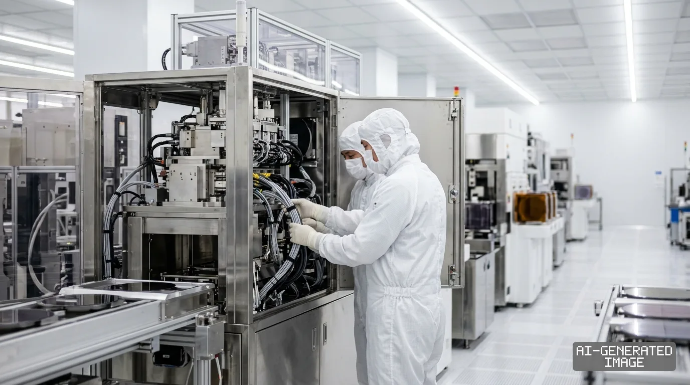
TSMC Urges HBM Makers to Adopt X-Ray Friendly Chip Design for Advanced Packaging
Zhihua Zou told a Taipei forum that buried defects in multi-layer stacks require memory redesigns to prevent radiation damage during high-speed inline scans.

Taiwan Semiconductor Manufacturing Co. urged memory makers on Sept. 4 to modify future chip architectures for non-destructive X-ray inspection, citing rising defect risks in multi-layer advanced packaging.
The foundry packages graphics processors with high-bandwidth memory for artificial intelligence accelerators. Its Chip-on-Wafer-on-Substrate platform connects multiple memory cubes around a central processor using a silicon interposer.
Zhihua Zou, packaging metrology director at TSMC, presented the appeal at the Semicon Taiwan forum in Taipei, Taiwan. He said the structural density of new packaging platforms strains standard defect detection tools.
Advanced packaging stacks have expanded from eight to 12 memory dies, with 16-layer configurations scheduled for commercial deployment. Each additional layer multiplies the microbumps and through-silicon vias embedded inside the package.
Hidden interconnect flaws now create severe assembly bottlenecks. Microbump bridging, solder voids and cracked vias sit deep within the silicon stacks where traditional optical inspection tools cannot see them.
Foundries must detect these buried flaws before completing final assembly. Defective interconnects can render an entire multi-chip module unusable, destroying expensive graphic computing dies placed on the same substrate.
Non-destructive inspection requires three-dimensional X-ray computed tomography and laminography. These systems penetrate dense silicon to generate cross-sectional views of microbumps without cutting the package open.
High-energy radiation introduces operational vulnerabilities into memory hardware. Dynamic random-access memory storage cells rely on delicate capacitors that lose stored electric charges when exposed to ionizing radiation.
Cumulative X-ray exposure during manufacturing inspection can induce bit errors, threshold voltage shifts and permanent physical damage. Memory chips lose operational reliability if inspection beams exceed specific radiation thresholds.
TSMC wants memory suppliers to incorporate radiation-tolerant structures into their silicon. Zou said chip layouts should include dedicated scan paths and shielding layers that protect sensitive bit lines during inline scanning.
The foundry also called for standardized fiducial marks and uniform metal density patterns. Consistent metal distribution allows X-ray inspection software to reconstruct internal images faster without creating visual artifacts.
Foundry integration demands have started reshaping front-end memory circuit development. Packaging constraints previously remained separate from wafer design rules, but three-dimensional integration has forced both disciplines to merge.
Suppliers must balance structural X-ray penetration against cell stability. Memory dies need low-density material pathways that let inspection beams pass through without demanding higher radiation power.
Neither Samsung Electronics nor SK hynix has issued formal statements regarding the TSMC proposal. Micron Technology has also refrained from publishing an official corporate response.
The three memory producers evaluate standalone X-ray inspection equipment on pilot production lines. Suppliers currently work with toolmakers including SEC Co., Techvalley and Rigaku Corp. to test inline scanning systems.
The memory industry operates without standardized design guidelines for radiation tolerance. Neither JEDEC nor international standards bodies have published binding rules for X-ray testable memory dies.
Component loss carries high financial consequences on advanced packaging lines. An AI processor package contains up to eight memory cubes surrounding two logic dies on a single interposer.
A single unspotted solder bridge inside one memory stack forces the assembler to scrap the entire finished device. Such failures eliminate thousands of dollars in silicon value at the final manufacturing gate.
Inline inspection tools must run at commercial production speeds. Packaging fabs process thousands of wafers each month, leaving only seconds to complete non-destructive imaging on each component.
Laboratory CT scanners require hours to capture high-resolution images of dense silicon packages. Inline equipment must deliver equal resolution within seconds to prevent assembly line stoppages.
Denser 16-layer memory stacks compound imaging difficulty. Thick stacks of silicon and copper interconnects disperse X-ray beams, forcing scanners to increase radiation intensity to capture readable images.
Foundry packaging capacity remains heavily allocated to top accelerator developers. TSMC has expanded its advanced packaging lines across western Taiwan to meet sustained server hardware orders.
Korean memory suppliers continue heavy capital investments to expand high-bandwidth memory capacity. SK hynix and Samsung Electronics have allocated substantial fabrication space to fifth-generation HBM3E and next-generation HBM4 lines.
The transition to HBM4 introduces custom base dies manufactured on advanced foundry logic nodes. Logic base dies increase circuit complexity and raise overall sensitivity to inspection radiation.
Equipment vendors have started developing low-dose X-ray tubes and artificial intelligence reconstruction algorithms. These software platforms reconstruct high-resolution images from lower radiation doses to minimize cell damage.
Metrology tool developers also build dual-energy detectors that distinguish between solder composition and copper pillars without increasing beam dwell time.
Foundries and memory makers have not set joint deadlines to implement unified X-ray design rules. Memory vendors continue inline tool qualifications while assessing the engineering cost of layout modifications.
Impact map
How this development propagates across the region and out to global buyers.
| Event | Korea | China | Japan | Global impact |
|---|---|---|---|---|
| X-ray design mandate | memory redesign burden | no direct access | inspection equipment demand | AI packaging yield risk |
In this story
- Companies
- TSMCSK hynixSamsung ElectronicsMicron Technology
- Tickers
- 2330.TW000660.KS005930.KSMU
- Policy
- Economic Security
- Impact
- Supply ChainCapexCost Structure
Track every Economic Security development →
Related briefings
- High-purity hydrogen peroxide supply chains face regional bottlenecks across East Asian fabs [90 characters] Also on Micron Technology, TSMC, SK hynix
- Micron taps TSMC for custom HBM4E memory, taking on SK hynix Also on Micron Technology, TSMC, SK hynix
- SK hynix validates HBM5 with TSMC on next-generation CoWoS Also on Micron Technology, TSMC, SK hynix
- Samsung narrows SK hynix HBM lead as HBM4 shipments expand Also on Micron Technology, TSMC, SK hynix
Sources
Reporting
Confidence: medium — how we grade this
The documents behind this briefing are linked above. East Asia Brief produces its English text with AI assistance under human editorial review, and does not translate or republish other outlets' articles. See our methodology and AI policy. Spotted an error? Tell us.
The Morning Brief
What changed in Korean, Chinese and Japanese industry overnight — and what it means for your supply chain. One email, weekday mornings, US time. Free.
The Morning Brief is in preparation. Leave your address and we will write to you once — when the first issue is ready. Nothing before that.