SK hynix honors Onto Innovation for advanced HBM inspection
The US toolmaker was the sole supplier recognized for technology achievement after deploying its Dragonfly G5 system to catch subsurface defects in stacked memory dies.
Onto Innovation announced Oct. 12, 2026, that it received the Best Partner Award for technology achievement from SK hynix for identifying subsurface defects during high-bandwidth memory production.
The award recognizes inspection systems used to prevent yield loss as memory manufacturers assemble complex multi-layer die stacks for artificial intelligence compute engines.
Global high-bandwidth memory capacity will expand by greater than 50% by 2027 to meet server demand, according to TrendForce data cited in the release.
SK hynix presented the honor during its 25th Anniversary Partners Day on Sept. 28, 2026, an annual recognition event held by the chipmaker's Co-Growth Council.
SK hynix named Onto Innovation as the only supplier honored for technology achievement during the ceremony, citing joint progress in defect prevention and metrology systems.
SK hynix Chief Executive Officer Kwak Noh-jung presented the award in person to Ryan Hwang, regional general manager of Onto Innovation Korea.
Close engineering work between the two firms helped fab lines identify hidden flaws that damage production yields, Onto Innovation Chief Executive Officer Mike Plisinski said.
Rapid changes in memory architecture require flexible inspection systems that adapt across successive generations of high-bandwidth memory, Plisinski said.
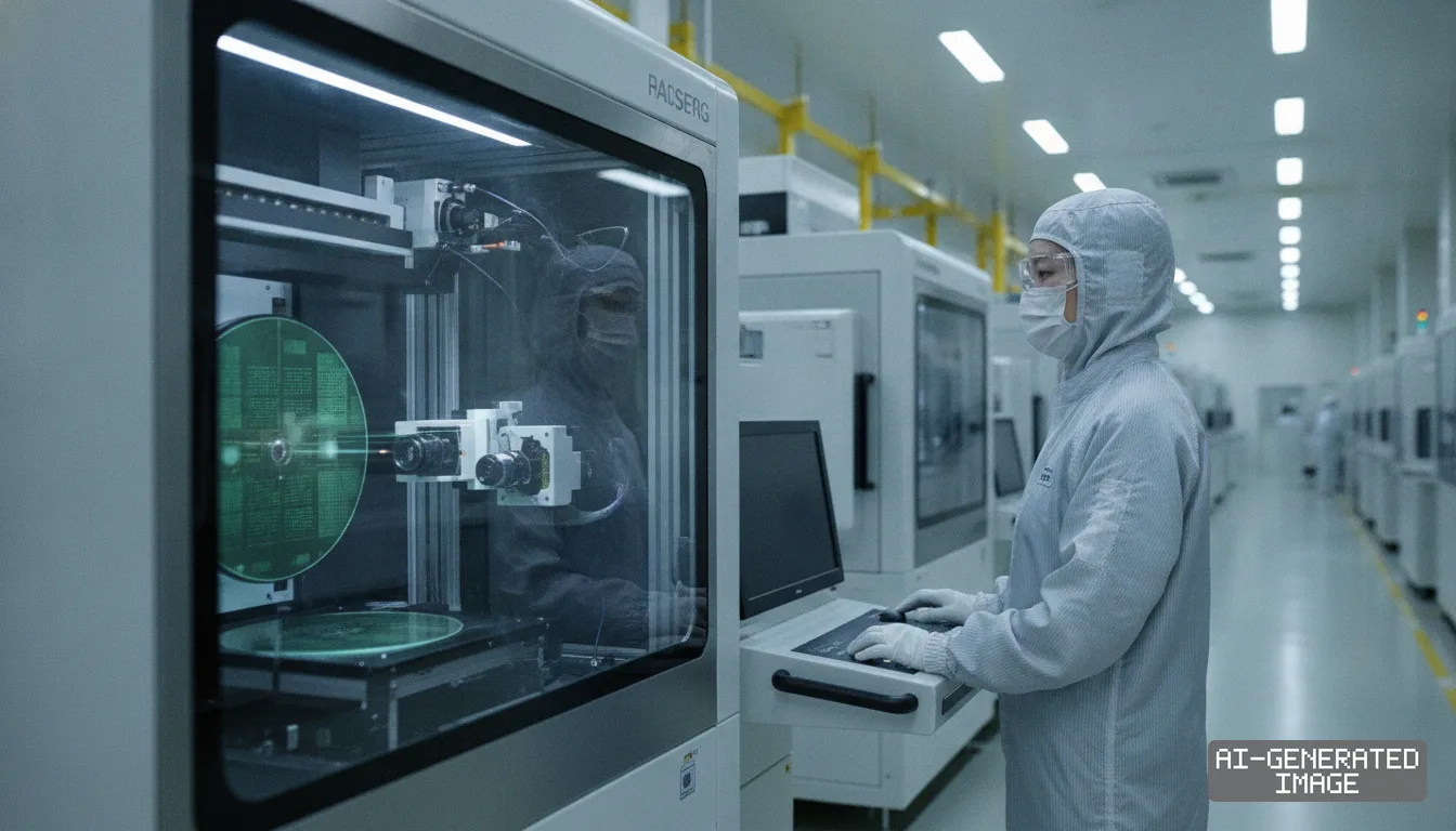
The recognition centers on Onto Innovation's Dragonfly G5 system, a specialized optical inspection tool deployed in advanced packaging facilities.
The system provides inline process control by detecting submicron defects down to 150 nanometers across heterogeneous integration steps, according to tool specifications.
The Dragonfly G5 platform operates at more than three times the wafer throughput of earlier inspection models, according to company technical documentation.
Onto Innovation integrated multi-angle illumination channels into the tool to raise signal-to-noise ratios when scanning faint optical flaws beneath wafer surfaces.
The optical hardware pairs with artificial intelligence algorithms to sort genuine defects from surface noise during high-speed wafer sweeps, the company said.
Process control challenges have grown more acute as the memory industry transitions from eight-layer stacks to 12-high and 16-high configurations.
Taller stacks require grinding dynamic random-access memory wafers to extreme thinness before stacking, leaving silicon dies fragile during subsequent handling.
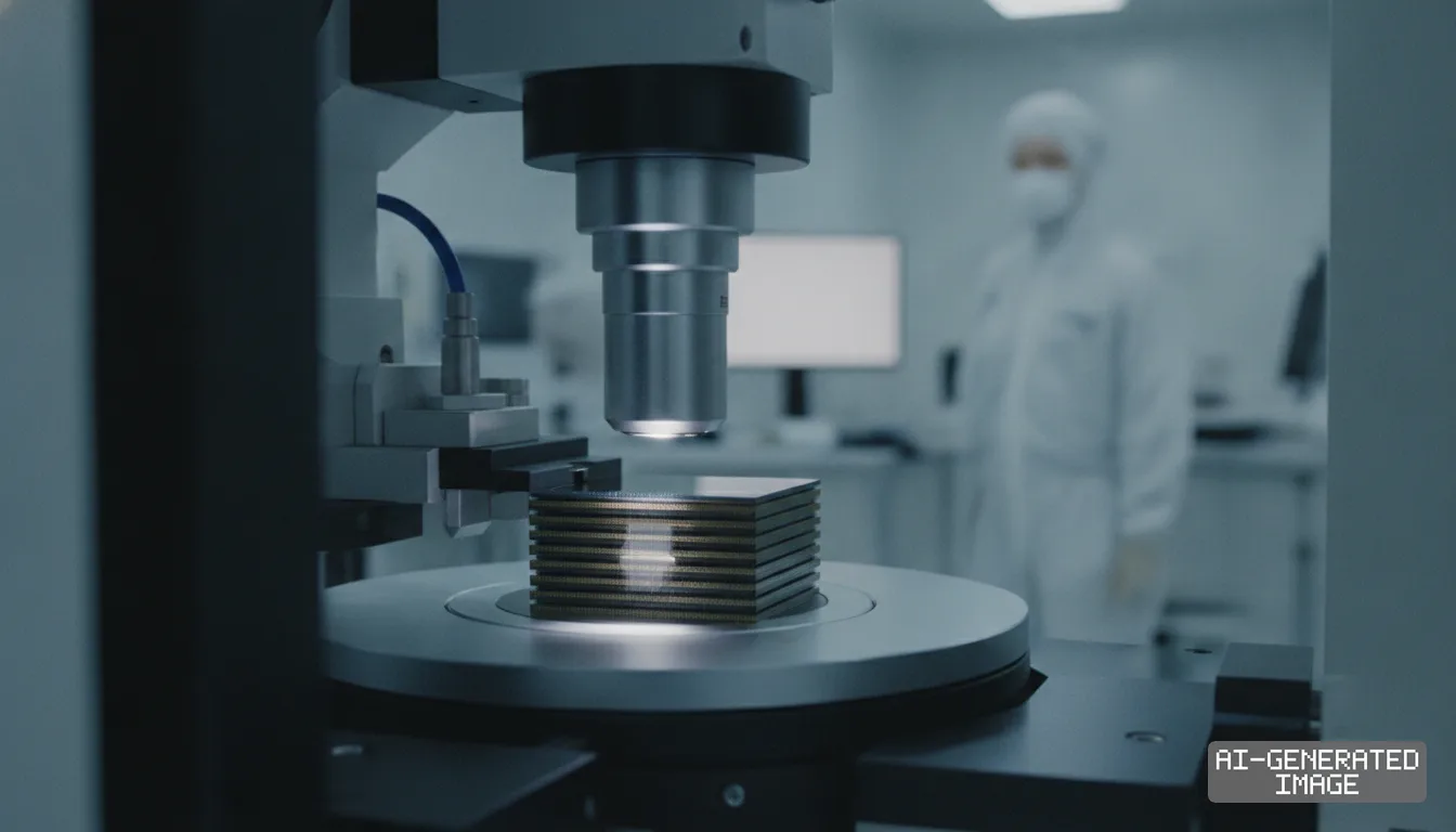
Subsequent assembly steps such as temporary bonding, wafer thinning and thermal compression introduce mechanical stress that causes micro-cracks inside the silicon.
Subsurface cracks often evade conventional surface-scan inspection tools, remaining undetected until final electrical package testing, according to packaging engineers.
Detecting cracks after final packaging destroys the entire stack of 12 or 16 premium dies, generating severe financial write-downs on advanced packaging lines.
Inline optical metrology allows SK hynix to catch damaged dies before thermocompression bonding, protecting expensive assemblies from compound defect propagation.
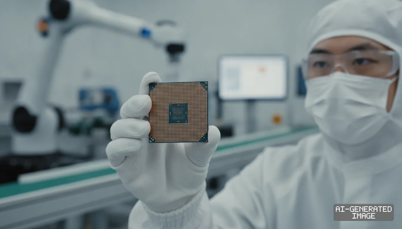
SK hynix has led shipments of fifth-generation HBM3E memory modules, serving as the primary supplier to Nvidia accelerated computing hardware.
The memory maker is ramping 12-high HBM3E production volumes while completing design verification for upcoming 16-high memory cubes.
Each layer addition tightens thermal and mechanical tolerances, making defect metrology as critical to final margins as front-end lithography yields.
Onto Innovation, headquartered in Wilmington, Massachusetts, has expanded its equipment portfolio to target advanced wafer-level packaging and chiplet interconnects.
The company supplies inspection and metrology tools to leading foundries, logic manufacturers and memory suppliers expanding heterogeneous integration capacity.
Process control equipment demand has outpaced general fab tool spending as chipmakers invest heavily to raise yields on high-value artificial intelligence silicon.
The notice does not state the monetary value of equipment deliveries under the partnership, and SK hynix has not published a separate vendor award notice on its official newsroom.
Onto Innovation scheduled an analyst event for December 2026 to brief institutional investors on packaging market adoption and business operations.
The equipment supplier will also exhibit its advanced packaging inspection portfolio at the SEMICON Europa industry conference opening Nov. 10, 2026, in Munich.
Impact map
How this development propagates across the region and out to global buyers.
| Event | Korea | China | Japan | Global impact |
|---|---|---|---|---|
| HBM defect inspection deployment | SK hynix cuts compound yield loss in 12- and 16-high HBM packaging | memory fabs lack access to equivalent sub-150nm advanced packaging inspection | packaging materials makers align NCF thermal profiles with inline metrology | AI server supply chain stabilizes as HBM yield loss drops on multi-die assemblies |
In this story
- Companies
- Onto InnovationSK hynix
- Tickers
- ONTO000660.KS
- Exposed
- Nvidia
- Policy
- Economic Security
- Impact
- Supply ChainCost Structure
Track every Economic Security development →
Related briefings
- GlobalFoundries signs $2B TSMC packaging deal for AI chips Also on Nvidia, SK hynix, Cost Structure
- Samsung and SK hynix deploy cooling packaging on HBM4E chips Also on Nvidia, SK hynix, Cost Structure
- SK hynix and Samsung push 16-layer HBM4 as Nvidia caps Rubin at 12 dies Also on Nvidia, SK hynix, Cost Structure
- Samsung revamps HBM thermal packaging to challenge TSMC supply lead Also on Nvidia, SK hynix, Cost Structure
Sources
Reporting
Confidence: medium — how we grade this
The documents behind this briefing are linked above. East Asia Brief produces its English text with AI assistance under human editorial review, and does not translate or republish other outlets' articles. See our methodology and AI policy. Spotted an error? Tell us.
The Morning Brief
What changed in Korean, Chinese and Japanese industry overnight — and what it means for your supply chain. One email, weekday mornings, US time. Free.
The Morning Brief is in preparation. Leave your address and we will write to you once — when the first issue is ready. Nothing before that.